Intel(Intersil) ISL9012 Data Sheet
Summary
The ISL9012 is a high-performance dual Low Dropout Regulator (LDO) designed for powering critical circuits in demanding portable electronics. It provides two independently controllable, highly stable voltage outputs while maintaining an extremely low quiescent current (45µA). This datasheet details the device’s comprehensive technical specifications, including advanced features like high PSRR, Power-On-Reset (POR), and wide input/output voltage options. Ideal for engineers developing smart phones, PDAs, or medical handheld devices that require both reliable power regulation and ultra-low power consumption in a compact footprint.
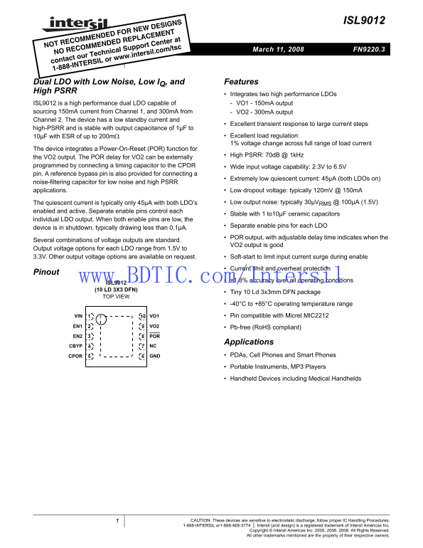
Page 1 Text Content
ISL9012
NOT RECOMMENDED FOR NEW DESIGNS
Data Sheet March 11, 2008 FN9220.3
NO RECOMMENDED REPLACEMENT contact our Technical Support Center at 1-888-INTERSIL or www.intersil.com/tsc
Dual LDO with Low Noise, Low IQ, and Features High PSRR
Integrates two high performance LDOs
ISL9012 is a high performance dual LDO capable of VO1 - 150m A output sourcing 150m A current from Channel 1, and 300m A from VO2 - 300m A output Channel 2. The device has a low standby current and
Excellent transient response to large current steps
high-PSRR and is stable with output capacitance of 1µF to
10µF with ESR of up to 200mΩ. Excellent load regulation: 1% voltage change across full range of load current
The device integrates a Power-On-Reset (POR) function for
High PSRR: 70d B @ 1k Hz
the VO2 output. The POR delay for VO2 can be externally programmed by connecting a timing capacitor to the CPOR Wide input voltage capability: 2.3V to 6.5V pin. A reference bypass pin is also provided for connecting a
Extremely low quiescent current: 45µA (both LDOs on)
noise-filtering capacitor for low noise and high PSRR applications. Low dropout voltage: typically 120m V @ 150m A
The quiescent current is typically only 45µA with both LDO’s Low output noise: typically 30µVRMS @ 100µA (1.5V)
enabled and active. Separate enable pins control each
Stable with 1 to10µF ceramic capacitors
individual LDO output. When both enable pins are low, the
Separate enable pins for each LDO
device is in shutdown, typically drawing less than 0.1µA.
POR output, with adjustable delay time indicates when the
Several combinations of voltage outputs are standard.
VO2 output is good
Output voltage options for each LDO range from 1.5V to 3.3V. Other output voltage options are available on request. Soft-start to limit input current surge during enable
Current limit and overheat protection
Pinout
www.BDTIC.com/Int ±1.8% accuracy over all operating conditions rsil
ISL9012 (10 LD 3X3 DFN)
Tiny 10 Ld 3x3mm DFN package
TOP VIEW
-40°C to +85°C operating temperature range VIN VO1 Pin compatible with Micrel MIC2212
EN1 VO2 Pb-free (Ro HS compliant)
EN2 POR
Applications
CBYP NC
CPOR GND PDAs, Cell Phones and Smart Phones
Portable Instruments, MP3 Players Handheld Devices including Medical Handhelds
CAUTION: These devices are sensitive to electrostatic discharge; follow proper IC Handling Procedures. 1-888-INTERSIL or1-888-468-3774 Intersil (and design) is a registered trademark of Intersil Americas Inc.
Copyright © Intersil Americas Inc. 2005, 2006. 2008. All Rights Reserved. All other trademarks mentioned are the property of their respective owners.
Page Summary Contents For Intel(Intersil) ISL9012 Data Sheet
Manual Details
| Brand | Intel |
|---|---|
| Pages | 11 |
| File Size | 220.99 KB |
| Published | May 30, 2026 |
Enter the captcha to get the download link:

Frequently Asked Questions
What is the operating temperature range?
The device operates in a -40°C to +85°C temperature range.
How stable are the LDO outputs regarding input voltage swings or load changes?
They offer excellent transient response, excellent load regulation (1% change), and high PSRR of 70dB @ 1kHz.
What is the typical quiescent current draw?
The quiescent current typically remains only 45µA when both LDOs are enabled and active.
Are there separate controls for each power output?
Yes, the device features separate enable pins (EN1 and EN2) to control each individual LDO output.