# A B C D E F G H I J K L M N O P Q R S T U V W X Y Z

Intel Intersil ISL6324A Data Sheet

Summary

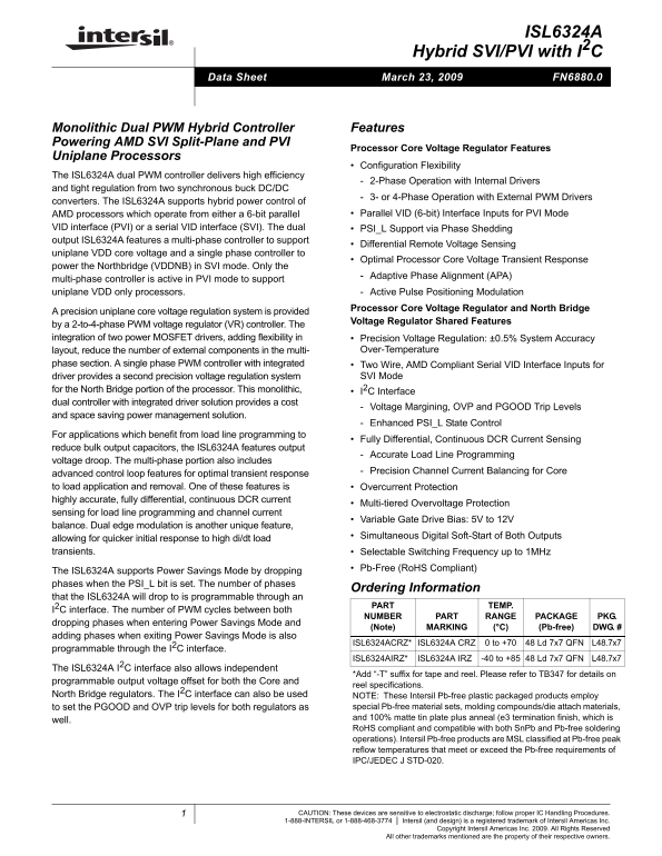
This manual provides comprehensive specifications for the ISL6324A, a high-efficiency monolithic dual PWM hybrid controller designed for modern processor core voltage regulation (AMD SVI/PVI). It ensures stable power delivery with precision up to ±0.5% accuracy and advanced features like adaptive phase alignment. Engineers can rely on this guide for detailed system integration, covering pinouts, electrical parameters, optimal PCB layout, and managing complex operational modes, making it essential for builders of sophisticated computing hardware.
📄 Preview PAGE OF 39

Page 1 Text Content

ISL6324A

Hybrid SVI/PVI with I2C

Data Sheet March 23, 2009 FN6880.0

Monolithic Dual PWM Hybrid Controller Features Powering AMD SVI Split-Plane and PVI

Processor Core Voltage Regulator Features

Uniplane Processors

Configuration Flexibility

The ISL6324A dual PWM controller delivers high efficiency

2-Phase Operation with Internal Drivers

and tight regulation from two synchronous buck DC/DC

3- or 4-Phase Operation with External PWM Drivers

converters. The ISL6324A supports hybrid power control of

AMD processors which operate from either a 6-bit parallel Parallel VID (6-bit) Interface Inputs for PVI Mode

VID interface (PVI) or a serial VID interface (SVI). The dual PSI_L Support via Phase Shedding output ISL6324A features a multi-phase controller to support

Differential Remote Voltage Sensing

uniplane VDD core voltage and a single phase controller to

Optimal Processor Core Voltage Transient Response

power the Northbridge (VDDNB) in SVI mode. Only the

Adaptive Phase Alignment (APA)

multi-phase controller is active in PVI mode to support uniplane VDD only processors. Active Pulse Positioning Modulation

Processor Core Voltage Regulator and North Bridge

A precision uniplane core voltage regulation system is provided

Voltage Regulator Shared Features

by a 2-to-4-phase PWM voltage regulator (VR) controller. The integration of two power MOSFET drivers, adding flexibility in Precision Voltage Regulation: ±0.5% System Accuracy

layout, reduce the number of external components in the multi- Over-Temperature

phase section. A single phase PWM controller with integrated Two Wire, AMD Compliant Serial VID Interface Inputs for

driver provides a second precision voltage regulation system SVI Mode

for the North Bridge portion of the processor. This monolithic, I2C Interface dual controller with integrated driver solution provides a cost

Voltage Margining, OVP and PGOOD Trip Levels

and space saving power management solution.

Enhanced PSI_L State Control

For applications which benefit from load line programming to

Fully Differential, Continuous DCR Current Sensing

reduce bulk output capacitors, the ISL6324A features output

Accurate Load Line Programming

voltage droop. The multi-phase portion also includes

Precision Channel Current Balancing for Core

advanced control loop features for optimal transient response to load application and removal. One of these features is Overcurrent Protection highly accurate, fully differential, continuous DCR current

Multi-tiered Overvoltage Protection

sensing for load line programming and channel current

Variable Gate Drive Bias: 5V to 12V

balance. Dual edge modulation is another unique feature,

Simultaneous Digital Soft-Start of Both Outputs

allowing for quicker initial response to high di/dt load transients. Selectable Switching Frequency up to 1MHz

Pb-Free (Ro HS Compliant)

The ISL6324A supports Power Savings Mode by dropping phases when the PSI_L bit is set. The number of phases

Ordering Information

that the ISL6324A will drop to is programmable through an

PART TEMP.

I2C interface. The number of PWM cycles between both

NUMBER PART RANGE PACKAGE PKG.

dropping phases when entering Power Savings Mode and

(Note) MARKING (°C) (Pb-free) DWG. #

adding phases when exiting Power Savings Mode is also

ISL6324ACRZ* ISL6324A CRZ 0 to +70 48 Ld 7x7 QFN L48.7x7

programmable through the I2C interface.

ISL6324AIRZ* ISL6324A IRZ -40 to +85 48 Ld 7x7 QFN L48.7x7

The ISL6324A I2C interface also allows independent

*Add “-T” suffix for tape and reel. Please refer to TB347 for details on

programmable output voltage offset for both the Core and

reel specifications.

North Bridge regulators. The I2C interface can also be used NOTE: These Intersil Pb-free plastic packaged products employ

to set the PGOOD and OVP trip levels for both regulators as special Pb-free material sets, molding compounds/die attach materials, and 100% matte tin plate plus anneal (e3 termination finish, which is

well.

Ro HS compliant and compatible with both Sn Pb and Pb-free soldering operations). Intersil Pb-free products are MSL classified at Pb-free peak reflow temperatures that meet or exceed the Pb-free requirements of IPC/JEDEC J STD-020.

CAUTION: These devices are sensitive to electrostatic discharge; follow proper IC Handling Procedures.

1-888-INTERSIL or 1-888-468-3774 Intersil (and design) is a registered trademark of Intersil Americas Inc.

Copyright Intersil Americas Inc. 2009. All Rights Reserved

All other trademarks mentioned are the property of their respective owners.

Page Summary Contents For Intel Intersil ISL6324A Data Sheet

Page 1 ISL6324A Hybrid SVI/PVI with I2C Data Sheet March 23, 2009 FN6880.0 Monolithic Dual PWM Hybrid Controller Features Powering AMD SVI Split-Plane and PVI Processor Core Voltage Regulator Features Unipla...
Page 2 ISL6324A Pinout ISL6324A HYBRID SVI AND PVI (48 LD QFN) TOP VIEW FB_NB PWM4 ISEN_NB+ PWM3 SDA PWROK VS EN P_ VID0/VFIXEN PHASE1 SC IS EN _N VID1/SEL UGATE1 IS EN 4+ VID2/SVD BOOT1 GND SE IS EN 4- VID3...
Page 3 ISL6324A Controller Block Diagram COMP_NBFB_NB NB_OVP SCL CORE_OVP I2C LGATE_NB DAC_OFS SDA E/A BOOT_NB MOSFET ISEN_NB+ CURRENT UV OV DRIVER NB_REF UGATE_NB SENSE LOGIC LOGIC ISEN_NB- RAMP PHASE_NB VD...
Page 4 ISL6324A Typical Application - SVI Mode FB VSEN COMP BOOT1 ISEN3+ BOOT1 ISEN3- UGATE1 UGATE1 PWM3 PHASE1 PHASE1 LGATE1 LGATE1 PWM1 APA PGND ISEN1- ISEN1+ ISL6614 PVCC1_2 +12V VCC VCC PVCC BOOT2 BOOT2 ...
Page 5 ISL6324A Typical Application - PVI Mode FB VSEN COMP BOOT1 BOOT1 ISEN3+ ISEN3- UGATE1 UGATE1 PWM3 PHASE1 PHASE1 LGATE1 LGATE1 APA PGND ISEN1- ISEN1+ ISL6614 PVCC1_2 VCC VCC BOOT2 BOOT2 UGATE2 UGATE2 G...
Page 6 ISL6324A Absolute Maximum Ratings Thermal Information Supply Voltage (VCC) . . . . . . . . . . . . . . . . . . . . . . . . -0.3V to +6.2V Thermal Resistance θJA (°C/W) θJC (°C/W) Supply Voltage (PVCC)...
Page 7 ISL6324A Electrical Specifications Recommended Operating Conditions (0°C to +70°C), Unless Otherwise Specified. Parameters with MIN and/or MAX limits are 100% tested at +25°C, unless otherwise specifi...
Page 8 ISL6324A Electrical Specifications Recommended Operating Conditions (0°C to +70°C), Unless Otherwise Specified. Parameters with MIN and/or MAX limits are 100% tested at +25°C, unless otherwise specifi...
Page 9 ISL6324A Functional Pin Description depending on the desired MOSFET gate-drive level. Decouple this pin with a quality 1.0µF ceramic capacitor. VID1/SEL PVCC_NB This pin selects SVI or PVI mode operat...
Page 10 ISL6324A ISEN1-, ISEN1+, ISEN2-, ISEN2+, ISEN3-, ISEN3+, DVC ISEN4-, and ISEN4+ The DVC pin is a buffered version of the reference to the error These pins are used for differentially sensing the corre...
Page 11 ISL6324A Operation The output capacitors conduct the ripple component of the inductor current. In the case of multi-phase converters, the The ISL6324A utilizes a multi-phase architecture to provide ca...
Page 12 ISL6324A To further improve the transient response, ISL6324A also INPUT-CAPACITOR CURRENT, 10A/DIV implements Intersil’s proprietary Adaptive Phase Alignment (APA) technique, which turns on all phases...
Page 13 ISL6324A switching frequency set by the resistor between the FS pin A simple R-C network across the inductor (R1, R2 and C) and ground. The PWM signals command the MOSFET extracts the DCR voltage, as ...
Page 14 ISL6324A current, IL, and the sensed current, ISEN, is driven by the value of the effective sense resistance, RISEN, and the DCR VCOMP PWM1 TO GATE of the inductor. MODULATOR CONTROL RAMP LOGIC IL ---...
Page 15 ISL6324A TABLE 1. 6-BIT PARALLEL VID CODES (Continued) TABLE 1. 6-BIT PARALLEL VID CODES (Continued) VID5 VID4 VID3 VID2 VID1 VID0 VREF VID5 VID4 VID3 VID2 VID1 VID0 VREF Serial VID Interface (SVI) Th...
Page 16 ISL6324A ENABLE PWROK V_SVI V_SVI METAL_VIDMETAL_VID VDD AND VDDNB VDDPWRGD VFIXEN FIGURE 7. SVI INTERFACE TIMING DIAGRAM: TYPICAL PRE-PWROK METAL VID START-UP PRE-PWROK METAL VID The VDD and VDDNB pl...
Page 17 ISL6324A to start-up VID values. Details of the SVI Bus protocol are If the PWROK input is de-asserted, then the controller steps provided in the AMD Design Guide for Voltage Regulator both VDD and VD...
Page 18 ISL6324A POWER SAVINGS MODE: PSI_L Voltage Regulation Bit 7 of the Serial VID code transmitted as part of the 8-bit The integrating compensation network shown in Figure 8 data phase over the SVI bus i...
Page 19 ISL6324A The magnitude of the spike is dictated by the ESR and ESL IDVC = IC RFB of the output capacitors selected. By positioning the no-load VSEN voltage level near the upper specification limit, a ...
Page 20 ISL6324A efficiency from the reduced freewheeling time of the lower Power-On Reset MOSFET body-diode conduction, and to prevent the upper and The ISL6324A requires VCC, PVCC1_2, and PVCC_NB lower MOSF...
Page 21 ISL6324A Phase Detection The ISEN3- and ISEN4- pins are monitored prior to soft-start to determine the number of active CORE channel phases. VCORE If ISEN4- is tied to VCC, the controller will configu...
Page 22 ISL6324A Overvoltage Protection The ISL6324A constantly monitors the sensed output voltage on the VSEN pin to detect if an overvoltage event occurs. When the output voltage rises above the OVP trip le...
Page 23 ISL6324A Sampling” on page 13 and “Channel-Current Balance” on zero. Once the regulator has completed soft-start, the page 14 for more detail on how the average current is overcurrent trip point will ...
Page 24 ISL6324A parameters and programmability of the Power Savings Mode feature. The parameters that can be adjusted through the I2C are: 1. Voltage Margining Offset: The DAC voltage can be offset in 25m V ...
Page 25 ISL6324A ISL6324A I2C Slave Address then sends a byte representing the data byte to be written into the desired register. The ISL6324A will respond with an All devices on the I2C bus must have a 7-Bit...
Page 26 ISL6324A then sends a new control byte with the R/W bit set to 1, POR rising threshold level, these registers can be changed indicating a read. The ISL6324A will then respond by at any time via the I2...
Page 27 ISL6324A Register Bit Definitions TABLE 8. BITS [5:0] REGISTER RGS1 and RGS2 (VOLTAGE MARGINING OFFSET) (Continued) The bits for RGS1 and RGS2 are utilized in the same manner by the ISL6324A (see Tabl...
Page 28 ISL6324A TABLE 8. BITS [5:0] REGISTER RGS1 and RGS2 Power Stages (VOLTAGE MARGINING OFFSET) (Continued) The first step in designing a multi-phase converter is to BIT5 BIT4 BIT3 BIT2 BIT1 BIT0 determin...
Page 29 ISL6324A Upper MOSFET losses can be divided into separate The bootstrap capacitor must have a maximum voltage components involving the upper-MOSFET switching times, rating above PVCC + 4V and its capa...
Page 30 ISL6324A components that connect to sensitive nodes or supply critical The total gate drive power losses are dissipated among the bypassing current and signal coupling.” on page 36 for thermal resisti...
Page 31 ISL6324A the R2 resistor for the North Bridge inductor RC filter is left 3. Calculate the value for the RSET resistor using unpopulated and K = 1. Equation 37:(Derived from Equation 18). DCRCORE K⋅ VI...
Page 32 ISL6324A 5. Calculate the value for the RSET resistor using Equation 44: Due to errors in the inductance and/or DCR it may be DCRCORE K⋅ VIN VCORE– VCORE necessary to adjust the value of R1 and R2 to ...
Page 33 ISL6324A RFB in this situation, please refer to “Compensation Without value of RC while observing the transient performance on an Loadline Regulation” on page 33. oscilloscope until no further improve...
Page 34 ISL6324A Case 2: C⋅⋅ ESR⋅ VP-P π⋅( )⋅ f0 C⋅ COMP -----------------------------------------------------------------⋅= RC RFB (EQ. 51) 0.66 VIN⋅ 0.66 VIN⋅ FB CC C1 π⋅( )2 f0 VP-P RFB C⋅⋅ ISL6324A R1 RFB...
Page 35 ISL6324A high-frequency capacitors allows them to support the output voltage as the current increases. Minimizing the ESR of the 10.61 1.035 f S( )log⋅( )–[ (EQ. 56) bulk capacitors allows them to sup...
Page 36 ISL6324A IN PU T- PA IT EN (I S/ 3-phase and two-phase designs respectively. Use the same approach for selecting the bulk capacitor type and number. Low capacitance, high-frequency ceramic capacitors ...
Page 37 ISL6324A The critical small components include the bypass capacitors The sense traces that connect the R-C sense components to (CFILTER) for VCC and PVCC, and many of the components each side of the o...
Page 38 ISL6324A CC RC CIN R3_2 FB VSEN CBOOT CBOOT BOOT1 R3_1C3 BOOT1 ISEN3+ ISEN3- UGATE1 UGATE1 PWM3 PHASE1 PHASE1 CAPA R1_1 C1 LGATE1 LGATE1 PGND ISEN1- ISEN1+ ISL6614 +12V V_CORE +5V PVCC1_2 +12V CFILTER...
Page 39 ISL6324A Package Outline Drawing L48.7x7 48 LEAD QUAD FLAT NO-LEAD PLASTIC PACKAGE Rev 4, 10/06 PIN #1 INDEX AREA PIN 1 INDEX AREA TOP VIEW 48X 0 . 40± 0 . 1 BOTTOM VIEW SEE DETAIL "X" 0 . 9...

Manual Details

Brand Intel
Pages 39
File Size 864.91 KB
Published May 29, 2026
104 views

Enter the captcha to get the download link:

captcha

Frequently Asked Questions

How does the ISL6324A handle different processor voltage modes?

It provides hybrid power control, managing processors that utilize either a 6-bit parallel VID interface (PVI) or a serial VID interface (SVI).

What advanced features improve load transient response time?

Features like Active Pulse Positioning Modulation and fully differential DCR current sensing help maintain voltage accuracy and reduce droop during sudden load changes.

Does the device support different soldering requirements?

Yes, it is RoHS compliant, using a termination finish compatible with both SnPb and modern Pb-free soldering operations.

How can I program the power consumption for light loads?

The ISL6324A supports Power Savings Mode by dropping phases when the PSI_L bit is set, a function adjustable through the IC interface.