Intel Intersil 82C284 Data Sheet
Summary
This clock generator system is designed to provide comprehensive timing control and clock signal distribution for 80C286 processors. It manages the generation of primary system clocks, reset outputs, and synchronized READY signals from both asynchronous and synchronous sources. The manual offers detailed functional diagrams and pin descriptions, guiding engineers in implementing precise bus synchronization and frequency switching necessary for complex embedded hardware designs.
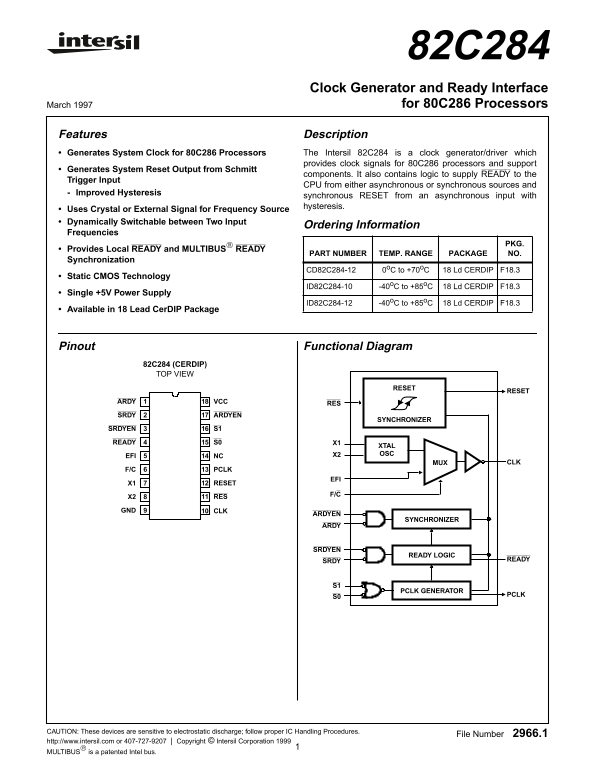
Page 1 Text Content
82C284 Clock Generator and Ready Interface March 1997 for 80C286 Processors
Features Description Generates System Clock for 80C286 Processors The Intersil 82C284 is a clock generator/driver which
provides clock signals for 80C286 processors and support
Generates System Reset Output from Schmitt
components. It also contains logic to supply READY to the
Trigger Input
CPU from either asynchronous or synchronous sources and
Improved Hysteresis
synchronous RESET from an asynchronous input with hysteresis.
Uses Crystal or External Signal for Frequency Source Dynamically Switchable between Two Input
Ordering Information
Frequencies
Provides Local READY and MULTIBUS READY
PART NUMBER TEMP. RANGE PACKAGE NO.
Synchronization
CD82C284-12 0o C to +70o C 18 Ld CERDIP F18.3
Static CMOS Technology
ID82C284-10 -40o C to +85o C 18 Ld CERDIP F18.3
Single +5V Power Supply
ID82C284-12 -40o C to +85o C 18 Ld CERDIP F18.3
Available in 18 Lead Cer DIP Package
Pinout Functional Diagram
82C284 (CERDIP) TOP VIEW
RESET
RESET
ARDY VCC RES SRDY ARDYEN
SYNCHRONIZER
SRDYEN S1
READY S0 X1
XTAL X2 OSC
EFI NC
MUX CLK
F/C PCLK
X1 RESET
X2 RES
GND CLK
ARDYEN
SYNCHRONIZER
SRDYEN
READY LOGIC
SRDY READY
PCLK GENERATOR
CAUTION: These devices are sensitive to electrostatic discharge; follow proper IC Handling Procedures.
File Number 2966.1
http://www.intersil.com or 407-727-9207 Copyright © Intersil Corporation 1999
MULTIBUS is a patented Intel bus.
Page Summary Contents For Intel Intersil 82C284 Data Sheet
Manual Details
| Brand | Intel |
|---|---|
| Pages | 11 |
| File Size | 72.19 KB |
| Published | May 30, 2026 |
Enter the captcha to get the download link:

Frequently Asked Questions
What is the purpose of this clock generator?
It generates system clock signals for 80C286 processors and supports multiple ready signal outputs.
How can I change the CLK frequency while running?
Use the F/C pin. Setting it HIGH allows the EFI input to drive CLK, enabling dynamic switching between frequencies.
What is the PCLK output?
PCLK provides a 50% duty cycle clock that is half the frequency of the main CLK signal. It will be in phase following the first bus cycle after processor reset.
Does the device handle system resets?
The active LOW RES input generates a robust system reset signal using a Schmitt trigger, which accepts asynchronous signals.