Intel(Intersil) ISL6269B User's Manual
Summary
This high-performance ISL6269B is a synchronous buck PWM controller engineered for sophisticated voltage regulation in demanding power applications. It ensures fast transient response and superior efficiency across wide input/output voltage ranges. The manual provides electrical engineers with comprehensive technical data, including functional block diagrams, typical application schematics, detailed operational parameters, and robust protection mechanisms needed to design highly reliable VRMs for advanced computing or networking hardware.
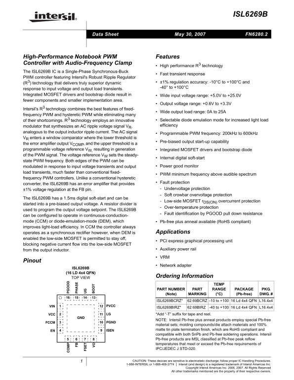
Page 1 Text Content
ISL6269B
May 30, 2007 FN6280.2Data Sheet
High-Performance Notebook PWM Features Controller with Audio-Frequency Clamp
High performance R3 technology
The ISL6269B IC is a Single-Phase Synchronous-Buck
Fast transient response
PWM controller featuring Intersil's Robust Ripple Regulator
(R3) technology that delivers truly superior dynamic ±1% regulation accuracy: -10°C to +100°C and -40° to +100°C
response to input voltage and output load transients. Integrated MOSFET drivers and bootstrap diode result in Wide input voltage range: +5.0V to +25.0V fewer components and smaller implementation area.
Output voltage range: +0.6V to +3.3V
Intersil’s R3 technology combines the best features of fixed-
Wide output load range: 0A to 25A
frequency PWM and hysteretic PWM while eliminating many
of their shortcomings. R3 technology employs an innovative Selectable diode emulation mode for increased light load modulator that synthesizes an AC ripple voltage signal VR, efficiency
analogous to the output inductor ripple current. The AC signal
Programmable PWM frequency: 200k Hz to 600k Hz
VR enters a window comparator where the lower threshold is
Pre-biased output start-up capability
the error amplifier output VCOMP, and the upper threshold is a programmable voltage reference VW, resulting in generation Integrated MOSFET drivers and bootstrap diode of the PWM signal. The voltage reference VW sets the steady-
Internal digital soft-start
state PWM frequency. Both edges of the PWM can be
modulated in response to input voltage transients and output Power good monitor
load transients, much faster than conventional fixed-
PWM minimum frequency above audible spectrum
frequency PWM controllers. Unlike a conventional hysteretic
Fault protection
converter, the ISL6269B has an error amplifier that provides
±1% voltage regulation at the FB pin. Undervoltage protection Soft crowbar overvoltage protection
The ISL6269B has a 1.5ms digital soft-start and can be
Low-side MOSFET r DS(ON) overcurrent protection
started into a pre-biased output voltage. A resistor divider is
Over-temperature protection
used to program the output voltage setpoint. The ISL6269B
Fault identification by PGOOD pull down resistance
can be configured to operate in continuous-conduction- mode (CCM) or diode-emulation-mode (DEM), which Pb-free plus anneal available (Ro HS compliant) improves light-load efficiency. In CCM the controller always
operates as a synchronous rectifier however, when DEM is Applications
enabled the low-side MOSFET is permitted to stay off,
PCI express graphical processing unit
blocking negative current flow into the low-side MOSFET
from the output inductor. Auxiliary power rail VRM
Pinout
Network adapter
ISL6269B (16 LD 4x4 QFN)
Ordering Information
TOP VIEW
TEMP PART NUMBER PART RANGE PACKAGE PKG. (Note) MARKING (°C) (Pb-free) DWG. #
ISL6269BCRZ* 62 69BCRZ -10 to +100 16 Ld 4x4 QFN L16.4x4
VIN PVCC
ISL6269BIRZ* 62 69BIRZ -40 to +100 16 Ld 4x4 QFN L16.4x4
VCC LG *Add “-T” suffix for tape and reel.
NOTE: Intersil Pb-free plus anneal products employ special Pb-free
FCCM PGND
material sets; molding compounds/die attach materials and 100% ISEN matte tin plate termination finish, which are Ro HS compliant and
compatible with both Sn Pb and Pb-free soldering operations. Intersil Pb-free products are MSL classified at Pb-free peak reflow temperatures that meet or exceed the Pb-free requirements of IPC/JEDEC J STD-020.
CAUTION: These devices are sensitive to electrostatic discharge; follow proper IC Handling Procedures.
1-888-INTERSIL or 1-888-468-3774 Intersil (and design) is a registered trademark of Intersil Americas Inc. Copyright Intersil Americas Inc. 2006, 2007. All Rights Reserved All other trademarks mentioned are the property of their respective owners.
Page Summary Contents For Intel(Intersil) ISL6269B User's Manual
Manual Details
| Brand | Intel |
|---|---|
| Pages | 14 |
| File Size | 315.87 KB |
| Published | May 31, 2026 |
Enter the captcha to get the download link:
