# A B C D E F G H I J K L M N O P Q R S T U V W X Y Z

Intel Intersil ISL6144 Five-Voltage Monitor Specifications Manual

Summary

This controller provides advanced fault tolerance for critical power distribution systems by acting as an ORing MOSFET solution. Ideal for engineers designing high-reliability equipment—such as network servers and data center infrastructure—it ensures continuous operation by detecting faults, isolating shorts in fast (<300ns) bursts, and managing multiple power sources. The manual details its wide operating range (+10V to +75V), superior switching performance compared to traditional diodes, and application recommendations for robust, redundant UPS and power path designs.
📄 Preview PAGE OF 29

Page 1 Text Content

ISL6144

Data Sheet February 15, 2007 FN9131.3

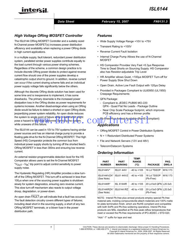
High Voltage ORing MOSFET Controller Features The ISL6144 ORing MOSFET Controller and a suitably sized Wide Supply Voltage Range +10V to +75V N-Channel power MOSFET(s) increases power distribution

Transient Rating to +100V

efficiency and availability when replacing a power ORing diode

in high current applications. Reverse Current Fault Isolation In a multiple supply, fault tolerant, redundant power distribution Internal Charge Pump Allows the use of N-Channel MOSFET

system, paralleled similar power supplies contribute equally to the load current through various power sharing schemes. HS Comparator Provides Very Fast <0.3µs Response Regardless of the scheme, a common design practice is to Time to Dead Shorts on Sourcing Supply. HS Comparator include discrete ORing power diodes to protect against reverse also has Resistor-adjustable Trip Level current flow should one of the power supplies develop a

HR Amplifier allows Quiet, <100µs MOSFET Turn-off for

catastrophic output short to ground. In addition, reverse current

Power Supply Slow Shut Down

can occur if the current sharing scheme fails and an individual

Open Drain, Active Low Fault Output with 120µs Delay

power supply voltage falls significantly below the others.

Provided in Packages Compliant to UL60950 (UL1950)

Although the discrete ORing diode solution has been used for

Creepage Requirements

some time and is inexpensive to implement, it has some drawbacks. The primary downside is the increased power QFN Package: dissipation loss in the ORing diodes as power requirements for Compliant to JEDEC PUB95 MO-220 systems increase. Another disadvantage when using an ORing QFN - Quad Flat No Leads - Package Outline diode would be failure to detect a shorted or open ORing diode, Near Chip Scale Package footprint, which improves jeopardizing power system reliability. An open diode reduces PCB efficiency and has a thinner profile the system to single point of failure while a diode short might

Pb-Free Plus Anneal Available (Ro HS Compliant)

pose a hazard to technical personnel servicing the system

www.BDTIC.com/Intersil while unaware of this failure.

Applications

The ISL6144 can be used in 10V to 75V systems having similar

ORing MOSFET Control in Power Distribution Systems

power sources and has an internal charge pump to provide a

N + 1 Redundant Distributed Power Systems

floating gate drive for the N-Channel ORing MOSFET. The High Speed (HS) Comparator protects the common bus from File and Network Servers (12V and 48V) individual power supply shorts by turning off the shorted feed’s

Telecom/Datacom Systems

ORing MOSFET in less than 300ns and ensuring low reverse current.

Ordering Information

An external resistor-programmable detection level for the HS

TEMP.

Comparator allows users to set the N-Channel MOSFET

PART PART RANGE PKG.

“VOUT - VIN” trip point to adjust control sensitivity to power NUMBER MARKING (°C) PACKAGE DWG. supply noise.

ISL6144IV* ISL61 44IV -40 to +105 16 Ld TSSOP M16.173

The Hysteretic Regulating (HR) Amplifier provides a slow turn-

ISL6144IVZA* ISL61 44IVZ -40 to +105 16 Ld TSSOP M16.173

off of the ORing MOSFET. This turn-off is achieved in less than

(See Note) (Pb-Free)

100μs when one of the sourcing power supplies is shutdown

slowly for system diagnostics, ensuring zero reverse current. ISL6144IR* ISL 6144IR -40 to +105 20 Ld 5x5 QFN L20.5x5

This slow turn-off mechanism also reacts to output voltage

ISL6144IRZA* ISL6144 IRZ -40 to +105 20 Ld 5x5 QFN L20.5x5

droop, degradation, or power-down.

(See Note) (Pb-Free)

An open drain FAULT pin will indicate that a fault has occurred.

NOTE: Intersil Pb-free plus anneal products employ special Pb-free

The fault detection circuitry covers different types of failures; material sets; molding compounds/die attach materials and 100% matte

including dead short in the sourcing supply, a short of any two tin plate termination finish, which are Ro HS compliant and compatible with both Sn Pb and Pb-free soldering operations. Intersil Pb-free

ORing MOSFET terminals, or a blown fuse in the power

products are MSL classified at Pb-free peak reflow temperatures that

distribution path.

meet or exceed the Pb-free requirements of IPC/JEDEC J STD-020.

*Add “-T” suffix for tape and reel.

CAUTION: These devices are sensitive to electrostatic discharge; follow proper IC Handling Procedures. 1-888-INTERSIL or 1-888-468-3774 Intersil (and design) is a registered trademark of Intersil Americas Inc.

Copyright © Intersil Americas Inc. 2004, 2006-2007. All Rights Reserved All other trademarks mentioned are the property of their respective owners.

Page Summary Contents For Intel Intersil ISL6144 Five-Voltage Monitor Specifications Manual

Page 1 ISL6144 Data Sheet February 15, 2007 FN9131.3 High Voltage ORing MOSFET Controller Features The ISL6144 ORing MOSFET Controller and a suitably sized Wide Supply Voltage Range +10V to +75V N-Channel po...
Page 2 ISL6144 Pinouts ISL6144 ISL6144 (16 LD TSSOP) (20 LD 5x5 QFN) TOP VIEW TOP VIEW GATE VOUT VIN COMP VIN VOUT HVREF VSET HVREF COMP NC NC NC VSET NC NC NC NC NC NC NC NC NC NC GND FAULT Pin Descriptions...
Page 3 ISL6144 General Application Circuit AC/DC DC/DC GATE GATEVIN VIN VOUT VOUT ISL6144 ISL6144 HVREF COMP HVREF COMP FAULT FAULT VSET VSET GND GND www.BDTIC.com/Intersil AC/DC DC/DC N + 1 N + 1 GATE GATE ...
Page 4 ISL6144 Simplified Block Diagram SOURCE 2 10V TO 75V VIN GATE VOUT COMPHVREF ISL6144 R2 VSETFAULT GND * D1, D2 PARASITIC DIODES **F1, F2 FUSES COULD ALSO BE PLACED ON THE INPUT SIDE BEFORE THE VIN PIN...
Page 5 ISL6144 Absolute Maximum Ratings TA = +25°C Thermal Information VIN, VOUT . . . . . . . . . . . . . . . . . . . . . . . . . . . . . . . . -0.3V to +100V Thermal Resistance (Typical, Note 1) θJA (°C/W)...
Page 6 ISL6144 Electrical Specifications VIN = 48V, TA = -40°C to +105°C, Unless Otherwise Specified (Continued) PARAMETER SYMBOL TEST CONDITIONS MIN TYP MAX UNITS COMP Input Current ICOMP 1.1 µA (bias curre...
Page 7 ISL6144 The slow turn-off is achieved in two stages. The first stage The fault can be detected and isolated by using the ISL6144 starts with a slow turn-off action and lasts for up to 20µs. The and an...
Page 8 ISL6144 High Voltage Pass and Clamp Application Considerations A high voltage pass and clamping circuit prevents the high ORing MOSFET Selection output voltage from damaging the comparators in case of...
Page 9 ISL6144 MOSFET M2 or ORing Diode D2 will be conducting the full On the other hand, the most common failures caused by load current. Power loss across the ORing devices is: diode ORing include open cir...
Page 10 ISL6144 VOS(HS) is the voltage offset of HS Comparator. IA COMP CAPACITOR (C2) Placed between VOUT and COMP pins to provide filtering The duration of the reverse current pulse is a few hundred and dec...
Page 11 ISL6144 Typical Performance Curves and Waveforms (Continued) 6.000 75V HVREF(VZ) 5.875 1V/DIV 10V/DIV 5.750 VG 10V/DIV 10V AND 12V 5.500 IIN 10A/DIV TEMPERATURE (°C) FIGURE 9. HVREF VOLTAGE FIGURE 10....
Page 12 Typical Performance Curves and Waveforms (Continued) 2A/DIV 10V/DIV 2V/DIV 10V/DIV VIN2 VGS2 5V/DIV 5V/DIV 2A/DIV FIGURE 13. SLOW SPEED TURN-OFF, VIN = 48V, COMMON FIGURE 14. SLOW SPEED TURN-OFF, VIN ...
Page 13 ISL6144 Using the ISL6144EVAL1 High Voltage A circuit fault condition is indicated on an open drain FAULT pin. The fault detection circuitry covers different types of ORing MOSFET Controller Evaluatio...
Page 14 ISL6144 DC/DC CONVERTERS (NOT PART OF THE EVAL BOARD) ISL6144EVAL1 CONTROL BOARD FIGURE 16. TEST SETUP USING DC/DC MODULES ISL6144 Evaluation Board Overview other). ORing MOSFET’s gate drive voltage, ...
Page 15 ISL6144 Input Voltage Range (+10V to +75V) (depending on the output capacitance value of the power supply/module, a local loading resistor might be needed to The ISL6144 can operate in equipment with ...
Page 16 ISL6144 DC/DC Converter Power Board (not part of the Two Feed Parallel Evaluation ISL6144EVAL1 board) Two Feed parallel operation verification can be performed The DC/DC converter board consists of tw...
Page 17 ISL6144 charge pump circuitry starts functioning as the input voltage VIN = 12V; RESISTIVE LOAD = 5A, CGSEXT = 33n F at the VIN pin reaches a value around 8V. The gate voltage depends on the load curr...
Page 18 ISL6144 Gate Fast Turn-off Test t DELAY(HS) is the High Speed Comparator internal worst- case time delay. The setup in Figure 18 can be used to During normal operation, the ISL6144 provides gate drive...
Page 19 ISL6144 The ISL6144EVAL1 board has VTH(HS) of 55m V. It can be Input Voltage is falling at a slow rate (Figure 26, top scope changed if performance is found to be unacceptable with this shot shows a 2...
Page 20 ISL6144 Detection of Power Feed Faults Fault 3: MOSFET Gate to Source Dead Short The ISL6144 have two built-in mechanisms that monitor GATE voltage will be equal to VIN, GATE &lt;VIN + 0.37V and a vol...
Page 21 ISL6144 Fault 6: ORing FET Body Diode Conduction For example, in a 48V, 32A (1 + 1) redundant system with current sharing, using a Schottky diode as the ORing device (VIN - 0.41V &gt; VOUT). If the vo...
Page 22 ISL6144 This shows that worst-case failure scenario has to be Suppose PLoss = 1W in a D2PAK MOSFET, junction to accounted for when choosing the ORing MOSFET. In both ambient thermal resistance RθJA = ...
Page 23 ISL6144 TABLE 2. INPUT VOLTAGE = 12V TO 24V Just a reminder, this is not an operating scenario, but it is rather a fault scenario and should not occur frequently. As ILoad_Max MOSFET PART NUMBER expla...
Page 24 ISL6144 PRIME_PS START SET VTH(HS) = 55m V R1 = 499Ω GATE R2 = 47.5kΩ VIN VOUT ISL6144C1 R3 HVREF COMP VOUT FAULT OPERATE ALL FEEDS IN CURRENT SHARING MODE Q2 BACKUP_PS (VIN1 = VIN2 =...= VINn) VIN VO...
Page 25 ISL6144 PCB Layout Considerations SOURCE1 - TP1, TP17 The ISL6144EVAL1 uses a 4 layer PCB with 1oz external DRAIN1 - TP2, TP18 layers and 2oz internal layers, dedicated ground and power GATE1 - TP13 p...
Page 26 ISL6144 ISL6144EVAL1 Schematics DNP Q3 VAUX1 J1 EXTERNAL 5V FDB3632 VIN1 DRAIN1 SOURCE1 Q1 TP18 J4 TP17 GATE1 TP1 TP2 FROM PS1 AT AT TP13 VIN VOUT VAUX1 TP28 150n F VIN1 COMP HVREF R3 R2 TP11 ISL6144 ...
Page 27 ISL6144 Bill of Material TABLE 3. BILL OF MATERIALS COMPONENT NAME SIZE, VALUE, RATING DESCRIPTION/COMMENTS CONTROL BOARD BOM R1, R6 VTH(HS) Programming Resistor 499Ω, RNC55, 1/8W TH on EVAL board, co...
Page 28 ISL6144 Thin Shrink Small Outline Plastic Packages (TSSOP) M16.173 16 LEAD THIN SHRINK SMALL OUTLINE PLASTIC PACKAGE INDEX 0.25(0.010) BM AREA INCHES MILLIMETERS GAUGE SYMBOL MAX MIN MAX NOTESMIN -B- ...
Page 29 ISL6144 Quad Flat No-Lead Plastic Package (QFN) L20.5x5 Micro Lead Frame Plastic Package (MLFP) 20 LEAD QUAD FLAT NO-LEAD PLASTIC PACKAGE MILLIMETERS SYMBOL NOMINAL MAX NOTESMIN A3 0.20 REF 5.00 BSC D...

Manual Details

Brand Intel
Pages 29
File Size 784.95 KB
Published May 30, 2026
113 views

Enter the captcha to get the download link:

captcha

Frequently Asked Questions

What is the voltage range for the ISL6144 controller?

It supports a wide supply voltage range of +10V to +75V.

How does the High Speed (HS) Comparator protect the power bus?

It protects against catastrophic output shorts by turning off the shorted feed in less than 300ns.

What is the benefit of using the ISL6144 over discrete ORing diodes?

It provides a lower profile, improves PCB efficiency, and prevents single point failure compared to traditional diode solutions.

Does the controller offer slow turn-off functionality for diagnostics?

Yes, the Hysteretic Regulating (HR) Amplifier achieves a slow turn-off in less than 100µs for system diagnostics.