Fairchild NC7SZ10 TinyLogic UHS 3-Input NAND Gate Data Sheet
Summary
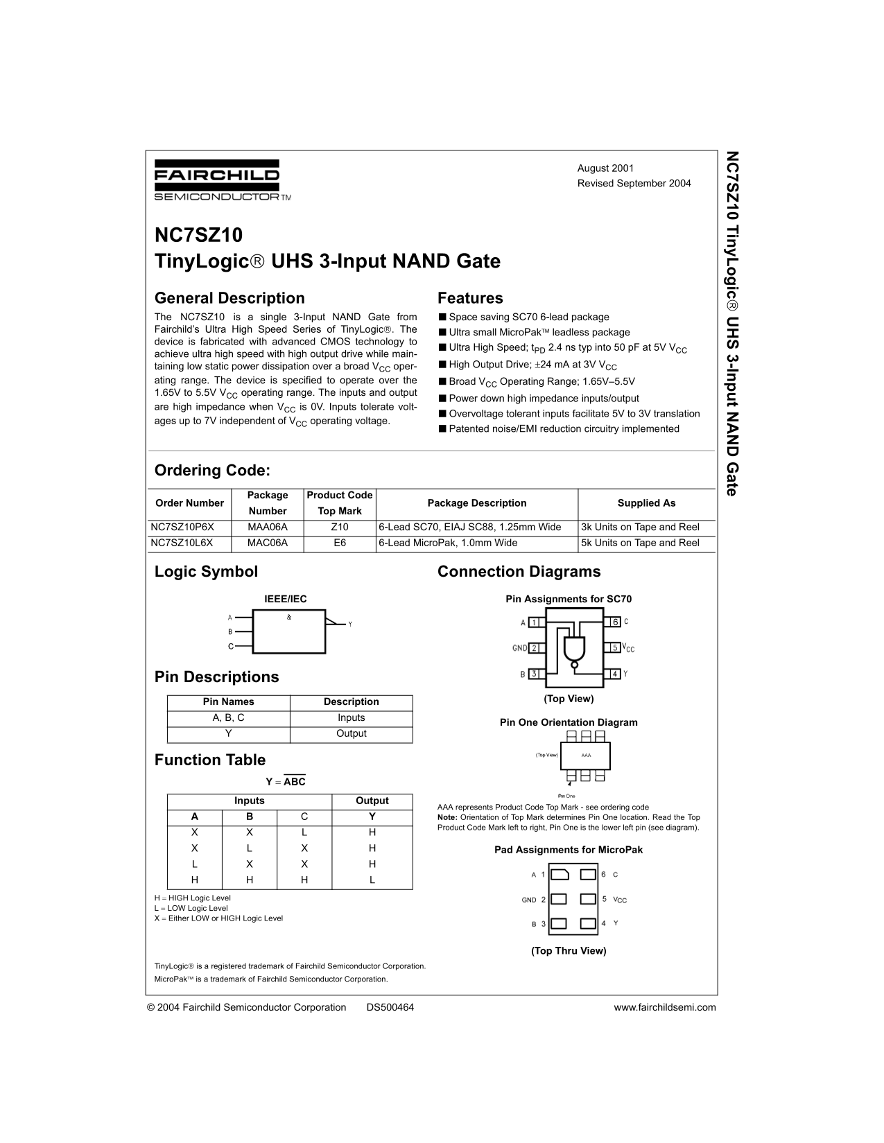
The NC7SZ10 is a high-speed, low-power 3-Input NAND Gate designed for advanced digital circuit applications. Optimized for reliable performance across a broad operating voltage range (1.65V–5.5V), it features ultra-high speed capabilities and robust EMI reduction circuitry. This technical documentation provides thorough specifications for electronics designers, including detailed electrical characteristics, package requirements (SC70/MicroPak), absolute maximum ratings, and timing parameters needed to integrate this efficient logic component into professional systems.
Page 1 Text Content
7S 10 Tin y L ic 3-In t N ate
August 2001 Revised September 2004
NC7SZ10 Tiny Logic UHS 3-Input NAND Gate General Description Features The NC7SZ10 is a single 3-Input NAND Gate from ■Space saving SC70 6-lead package Fairchild’s Ultra High Speed Series of Tiny Logic. The
■Ultra small Micro Pak leadless package
device is fabricated with advanced CMOS technology to
■Ultra High Speed; t PD 2.4 ns typ into 50 p F at 5V VCC
achieve ultra high speed with high output drive while main-
taining low static power dissipation over a broad VCC oper- ■High Output Drive; ±24 m A at 3V VCC
ating range. The device is specified to operate over the ■Broad VCC Operating Range; 1.65V–5.5V 1.65V to 5.5V VCC operating range. The inputs and output
■Power down high impedance inputs/output
are high impedance when VCC is 0V. Inputs tolerate volt-
■Overvoltage tolerant inputs facilitate 5V to 3V translation
ages up to 7V independent of VCC operating voltage.
■Patented noise/EMI reduction circuitry implemented
Ordering Code:
Package Product Code
Order Number Package Description Supplied As
Number Top Mark
NC7SZ10P6X MAA06A Z10 6-Lead SC70, EIAJ SC88, 1.25mm Wide 3k Units on Tape and Reel NC7SZ10L6X MAC06A E6 6-Lead Micro Pak, 1.0mm Wide 5k Units on Tape and Reel
Logic Symbol Connection Diagrams
IEEE/IEC Pin Assignments for SC70
Pin Descriptions
(Top View)
Pin Names Description A, B, C Inputs
Pin One Orientation Diagram
Output
Function Table
Y = ABC
Inputs Output
AAA represents Product Code Top Mark - see ordering code Note: Orientation of Top Mark determines Pin One location. Read the Top Product Code Mark left to right, Pin One is the lower left pin (see diagram).
Pad Assignments for Micro Pak
H = HIGH Logic Level L = LOW Logic Level X = Either LOW or HIGH Logic Level
(Top Thru View)
Tiny Logic is a registered trademark of Fairchild Semiconductor Corporation. Micro Pak is a trademark of Fairchild Semiconductor Corporation.
© 2004 Fairchild Semiconductor Corporation DS500464 www.fairchildsemi.com
Page Summary Contents For Fairchild NC7SZ10 TinyLogic UHS 3-Input NAND Gate Data Sheet
Manual Details
| Brand | Fairchild |
|---|---|
| Pages | 7 |
| File Size | 147.63 KB |
| Published | July 16, 2026 |
Enter the captcha to get the download link:

Frequently Asked Questions
What is the reliable operational voltage range for this NAND gate?
The device is specified to operate over a broad range of 1.65V–5.5V.
How fast does the gate perform under typical conditions?
At $5 ext{V}$, the typical propagation delay ($t_{PLH}$) into $50 ext{ pF}$ is $2.4 ext{ ns}$.
Are the gate inputs resistant to high voltages or noise?
Yes, they are overvoltage tolerant (up to 7V) and feature patented noise/EMI reduction circuitry.
What physical package options does this NAND gate come in?
It is supplied as either a 6-Lead SC70 (1.25mm Wide) or a MicroPak (1.0mm Wide) package.