Fairchild FDY6342L Integrated Load Switch Data Manual
Summary
The FDY6342L is a high-performance integrated load switch designed for compact power management in portable electronic equipment. Featuring extremely low On-Resistance and robust design, this device offers reliable ON/OFF switching capability while minimizing power loss. The manual provides comprehensive electrical characteristics, detailed operational specifications, and application guidelines necessary for engineers integrating efficient power solutions into their next generation of electronic devices.
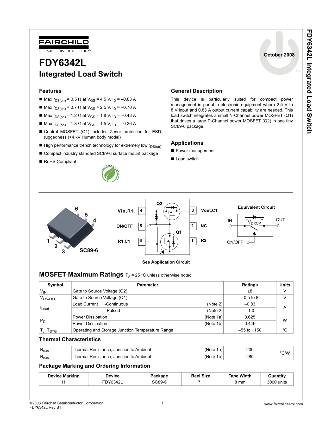
Page 1 Text Content
FD Y6342L Integrated Load Sw itch
October 2008
FDY6342L
Integrated Load Switch
Features General Description Max r DS(on) = 0.5 Ω at VGS = 4.5 V, ID = –0.83 A This device is particularly suited for compact power
management in portable electronic equipment where 2.5 V to
Max r DS(on) = 0.7 Ω at VGS = 2.5 V, ID = –0.70 A
8 V input and 0.83 A output current capability are needed. This Max r DS(on) = 1.2 Ω at VGS = 1.8 V, ID = –0.43 A load switch integrates a small N-Channel power MOSFET (Q1) that drives a large P-Channel power MOSFET (Q2) in one tiny
Max r DS(on) = 1.8 Ω at VGS = 1.5 V, ID = –0.36 A
SC89-6 package.
Control MOSFET (Q1) includes Zener protection for ESD ruggedness (>4 k V Human body model)
Applications
High performance trench technology for extremely low r DS(on)
Power management
Compact industry standard SC89-6 surface mount package
Load switch
Ro HS Compliant
Equivalent Circuit
3Vin,R1 Vout,C14
OUTIN
VDROP
ON/OFF NC
ON/OFF
SC89-6
See Application Circuit
MOSFET Maximum Ratings TA = 25 °C unless otherwise noted Symbol Parameter Ratings Units VIN Gate to Source Voltage (Q2) ±8
VON/OFF Gate to Source Voltage (Q1) –0.5 to 8 Load Current -Continuous (Note 2) –0.83
ILoad
-Pulsed (Note 2) –1.0 Power Dissipation (Note 1a) 0.625
Power Dissipation (Note 1b) 0.446 TJ, TSTG Operating and Storage Junction Temperature Range –55 to +150 °C
Thermal Characteristics
RθJA Thermal Resistance, Junction to Ambient (Note 1a)
RθJA Thermal Resistance, Junction to Ambient (Note 1b)
Package Marking and Ordering Information Device Marking Device Package Reel Size Tape Width Quantity
FDY6342L SC89-6 7 ’’ 8 mm 3000 units
www.fairchildsemi.com1©2008 Fairchild Semiconductor Corporation
FDY6342L Rev.B1
Page Summary Contents For Fairchild FDY6342L Integrated Load Switch Data Manual
Manual Details
| Brand | Fairchild |
|---|---|
| Pages | 5 |
| File Size | 212.99 KB |
| Published | July 06, 2026 |
Enter the captcha to get the download link:

Frequently Asked Questions
What package is the FDY6342L available in?
It comes in a compact industry standard SC89-6 surface mount package.
Is this load switch suitable for power management in portable equipment?
Yes, it is particularly suited for power management in portable electronic equipment.
What are the maximum operating temperatures and range?
The junction temperature operating range is –55 to +150 °C. The storage temperature range is –55 to +150 °C.
Does Q1 include protection against electrostatic discharge (ESD)?
Yes, the control MOSFET (Q1) includes Zener protection for ESD ruggedness (>4 kV Human body model).
When should I use external components with this device?
R2 and C1 can be added externally for additional in-rush current control.