Fairchild FDG6323L Integrated Load Switch Data Manual
Summary
This high-density load switch provides compact power management for low-power electronic equipment. It integrates two MOSFETs and Zener protection in a tiny SC70-6 package, making it ideal where space constraints are critical. The accompanying manual offers comprehensive technical data, including electrical characteristics, thermal modeling, and detailed application circuits, ensuring reliable implementation across various voltage and current demands. It is perfect for engineers designing compact, energy-efficient systems requiring precise switching control.
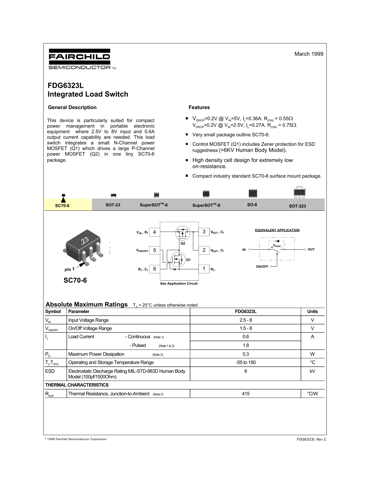
Page 1 Text Content
March 1999
FDG6323L Integrated Load Switch General Description Features
VDROP=0.2V @ VIN=5V, IL=0.36A. R(ON) = 0.55Ω
This device is particularly suited for compact
power management in portable electronic VDROP=0.2V @ VIN=2.5V, IL=0.27A. R(ON) = 0.75Ω.
equipment where 2.5V to 8V input and 0.6A
Very small package outline SC70-6.
output current capability are needed. This load switch integrates a small N-Channel power
Control MOSFET (Q1) includes Zener protection for ESD
MOSFET (Q1) which drives a large P-Channel
ruggedness (>6KV Human Body Model).
power MOSFET (Q2) in one tiny SC70-6 package. High density cell design for extremely low
on-resistance. Compact industry standard SC70-6 surface mount package.
SOT-23 Super SOTTM-6 Super SOTTM-8 SO-8
SOT-223SC70-6
EQUIVALENT APPLICATION
V , RIN V , COUT
VDROP+
V , COUT IN OUT
ON/OFFV
ON/OFF
pin R , C11 R2
SC70-6
See Application Circuit
Absolute Maximum Ratings TA = 25°C unless otherwise noted Symbol Parameter FDG6323L Units VIN Input Voltage Range 2.5 - 8 VON/OFF On/Off Voltage Range 1.5 - 8 I L Load Current - Continuous (Note 1) 0.6
- Pulsed (Note 1 & 3) 1.8
PD Maximum Power Dissipation (Note 2) 0.3 TJ,TSTG Operating and Storage Temperature Range -55 to 150 °C ESD Electrostatic Discharge Rating MIL-STD-883D Human Body k V
Model (100pf/1500Ohm)
THERMAL CHARACTERISTICS
RθJA Thermal Resistance, Junction-to-Ambient (Note 2) °C/W
© 1999 Fairchild Semiconductor Corporation FDG6323L Rev.C
Page Summary Contents For Fairchild FDG6323L Integrated Load Switch Data Manual
Manual Details
| Brand | Fairchild |
|---|---|
| Pages | 4 |
| File Size | 98.03 KB |
| Published | July 07, 2026 |
Enter the captcha to get the download link:

Frequently Asked Questions
What is the ideal application for this load switch?
It's suited for power management in electronic equipment where 2.5 V to 8 V input and up to 0.6A output current are needed.
How do I control the FET switching action (Q2)?
An external resistor R1 is required to turn Q2 off, although R2 can be used optionally for slew rate control.
What temperature range can it operate in?
The operating and storage temperature range is -55 to 150 °C.
Does this load switch have protection features?
Yes, it includes Zener protection for ESD and the main MOSFET (Q2).
How does the thermal resistance impact performance?
Thermal resistance (RthJA) accounts for junction-to-ambient transfer and changes based on circuit board design.