Fairchild FDG6342L Integrated Load Switch Data Sheet
Summary
Optimized for power management in portable electronics, this integrated load switch offers highly efficient and compact DC-DC switching capability within an SC70-6 package. It features low on-resistance ($r_{DS(on)}$) and integral Zener protection, making it ideal for managing loads in small electronic devices ranging from 2.5V to 8V. The manual provides comprehensive technical data, including maximum ratings, detailed electrical characteristics, thermal analysis, and application circuits necessary for engineers designing reliable, high-performance power systems.
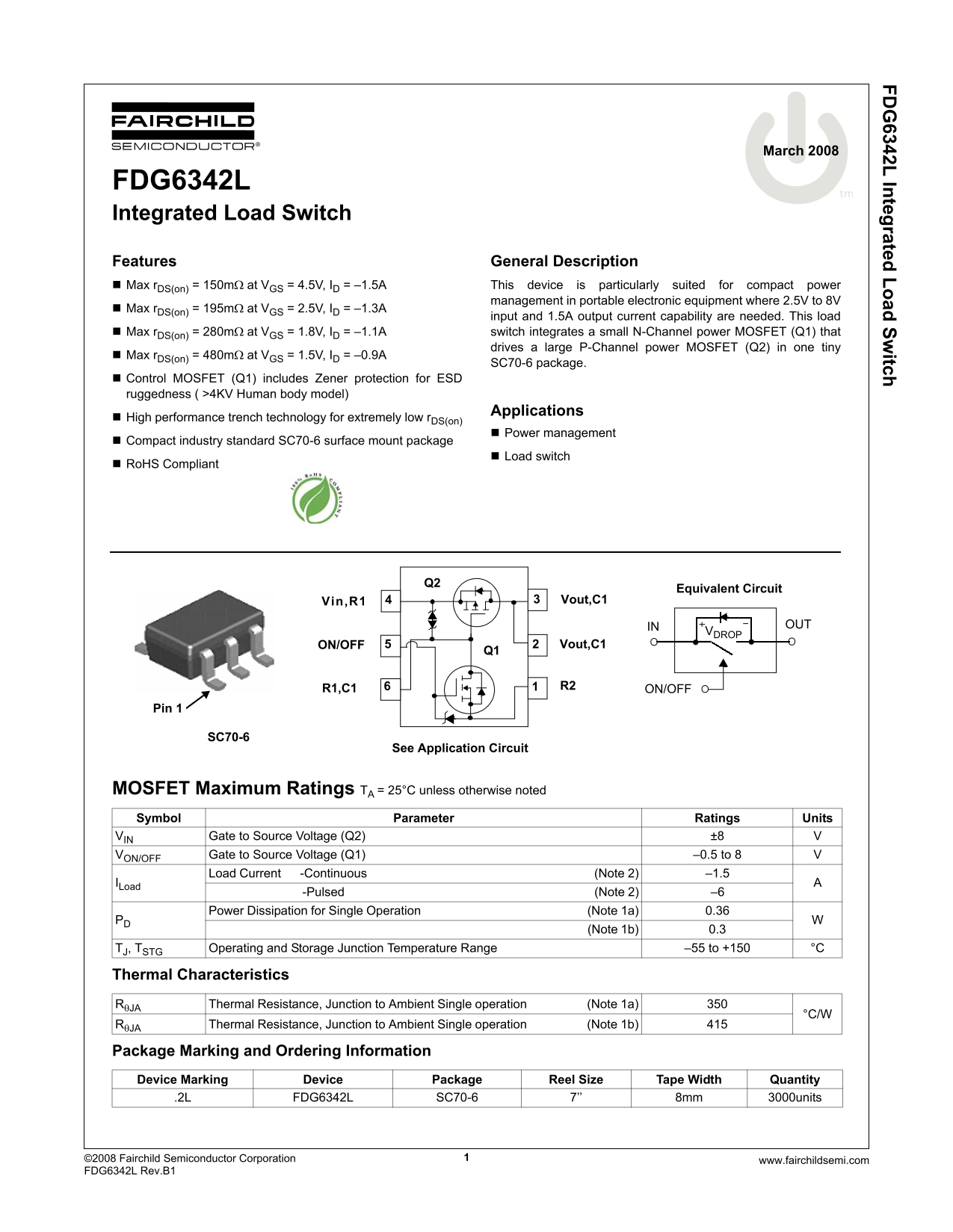
Page 1 Text Content
FD 6342L Integrated Load Sw itch
March 2008
FDG6342L
Integrated Load Switch
Features General Description Max r DS(on) = 150mΩ at VGS = 4.5V, ID = –1.5A This device is particularly suited for compact power
management in portable electronic equipment where 2.5V to 8V
Max r DS(on) = 195mΩ at VGS = 2.5V, ID = –1.3A
input and 1.5A output current capability are needed. This load Max r DS(on) = 280mΩ at VGS = 1.8V, ID = –1.1A switch integrates a small N-Channel power MOSFET (Q1) that drives a large P-Channel power MOSFET (Q2) in one tiny
Max r DS(on) = 480mΩ at VGS = 1.5V, ID = –0.9A
SC70-6 package.
Control MOSFET (Q1) includes Zener protection for ESD ruggedness ( >4KV Human body model)
Applications
High performance trench technology for extremely low r DS(on)
Power management
Compact industry standard SC70-6 surface mount package
Load switch
Ro HS Compliant
Equivalent Circuit
3Vin,R1 Vout,C14
OUTIN
VDROP
ON/OFF Vout,C1
ON/OFF
Pin 1
SC70-6
See Application Circuit
MOSFET Maximum Ratings TA = 25°C unless otherwise noted Symbol Parameter Ratings Units VIN Gate to Source Voltage (Q2) ±8
VON/OFF Gate to Source Voltage (Q1) –0.5 to 8 Load Current -Continuous (Note 2) –1.5
ILoad
-Pulsed (Note 2) –6 Power Dissipation for Single Operation (Note 1a) 0.36
(Note 1b) 0.3 TJ, TSTG Operating and Storage Junction Temperature Range –55 to +150 °C
Thermal Characteristics
RθJA Thermal Resistance, Junction to Ambient Single operation (Note 1a)
RθJA Thermal Resistance, Junction to Ambient Single operation (Note 1b)
Package Marking and Ordering Information Device Marking Device Package Reel Size Tape Width Quantity
.2L FDG6342L SC70-6 7’’ 8mm 3000units
©20 08 Fairchild Semiconductor Corporation www.fairchildsemi.com1 FD G6342L Rev.B1
Page Summary Contents For Fairchild FDG6342L Integrated Load Switch Data Sheet
Manual Details
| Brand | Fairchild |
|---|---|
| Pages | 4 |
| File Size | 193.68 KB |
| Published | July 15, 2026 |
Enter the captcha to get the download link:

Frequently Asked Questions
What are the maximum operating voltages supported by this load switch?
The device is suited for power management where 2.5V to 8V is needed.
How can I mitigate in-rush current when implementing the circuit?
For additional in-rush current control, R2 and C1 can be added externally.
Is this load switch approved for use in life support devices?
No; its use in life support systems requires the express written approval of Fairchild Semiconductor Corporation.
What is the resistance rating at 4.5V and -1.5A?
The maximum resistance (R) is specified as 150mΩ.