Fairchild FDG6322C Dual N & P Channel Digital FET Data Handbook
Summary
The FDG6322C is a dual N & P-Channel logic level enhancement mode field effect transistor (FET) engineered using high-cell density DMOS technology. Designed for low-voltage applications, it serves as an efficient replacement for bipolar digital transistors and small signal MOSFETs in 3V circuits. This technical datasheet provides comprehensive electrical characteristics, dynamic specifications, and thermal ratings for engineers and hardware designers.
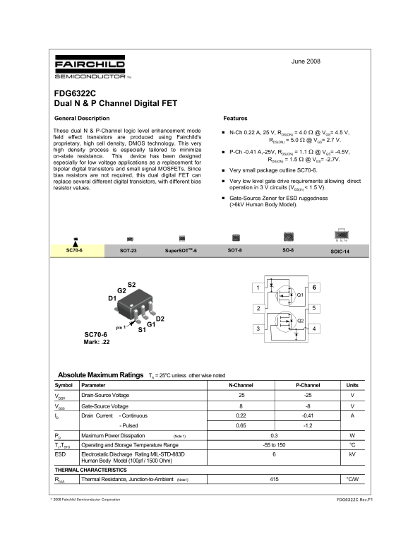
Page 1 Text Content
June 2008
FDG6322C Dual N & P Channel Digital FET General Description Features These dual N & P-Channel logic level enhancement mode
N-Ch 0.22 A, 25 V, RDS(ON) = 4.0 Ω @ VGS= 4.5 V,
field effect transistors are produced using Fairchild's
RDS(ON) = 5.0 Ω @ VGS= 2.7 V.
proprietary, high cell density, DMOS technology. This very high density process is especially tailored to minimize
P-Ch -0.41 A,-25V, RDS(ON) = 1.1 Ω @ VGS= -4.5V,
on-state resistance. This device has been designed
RDS(ON) = 1.5 Ω @ VGS= -2.7V.
especially for low voltage applications as a replacement for bipolar digital transistors and small signal MOSFETs. Since
Very small package outline SC70-6.
bias resistors are not required, this dual digital FET can
replace several different digital transistors, with different bias Very low level gate drive requirements allowing direct resistor values. operation in 3 V circuits (VGS(th) < 1.5 V). Gate-Source Zener for ESD ruggedness (>6k V Human Body Model).
SC70-6 Super SOTTM-6 SOIC-14SO-8SOT-8SOT-23
SC70-6 Mark: .22
Absolute Maximum Ratings TA = 25o C unless other wise noted Symbol Parameter N-Channel P-Channel Units VDSS Drain-Source Voltage 25 -25 V VGSS Gate-Source Voltage 8 -8 V
ID Drain Current - Continuous 0.22 -0.41 A - Pulsed 0.65 -1.2 PD Maximum Power Dissipation (Note 1) 0.3 W TJ,TSTG Operating and Storage Temperature Range -55 to 150 °C
ESD Electrostatic Discharge Rating MIL-STD-883D 6 k V
Human Body Model (100pf / 1500 Ohm)
THERMAL CHARACTERISTICS RθJA Thermal Resistance, Junction-to-Ambient (Note1) 415 °C/W
© 2008 Fairchild Semiconductor Corporation FDG6322C Rev.F1
Page Summary Contents For Fairchild FDG6322C Dual N & P Channel Digital FET Data Handbook
Manual Details
| Brand | Fairchild |
|---|---|
| Pages | 9 |
| File Size | 669.69 KB |
| Published | June 20, 2026 |
Enter the captcha to get the download link:

Frequently Asked Questions
What kind of technology is the DG6 dual FET built upon?
It uses proprietary, high cell density, DMOS technology.
Is this device suitable for low voltage applications?
Yes, it was designed especially for low voltage applications and can direct operate in 3 V circuits (V < 1.5 V).
What is the electrostatic discharge (ESD) rating?
The ESD rating is specified as 6kV according to MIL-STD-883D Human Body Model.
How does the thermal coupling factor work for this device?
R(JA) represents the sum of junction-to-case and case-to-ambient thermal resistance.