Fairchild FDG6318PZ Dual P-Channel, Digital FET Data Sheet
Summary
An efficient dual P-Channel MOSFET designed for reliable small signal and digital interfacing, making it ideal for low-voltage 3V circuits and bipolar transistor applications. This component features ultra-low on-state resistance in a compact SC-70-6 package. The accompanying technical manual provides comprehensive specifications covering all critical aspects of circuit design, including maximum ratings, dynamic switching characteristics, detailed thermal performance curves, and electrical parameters necessary for robust system integration by electronics engineers.
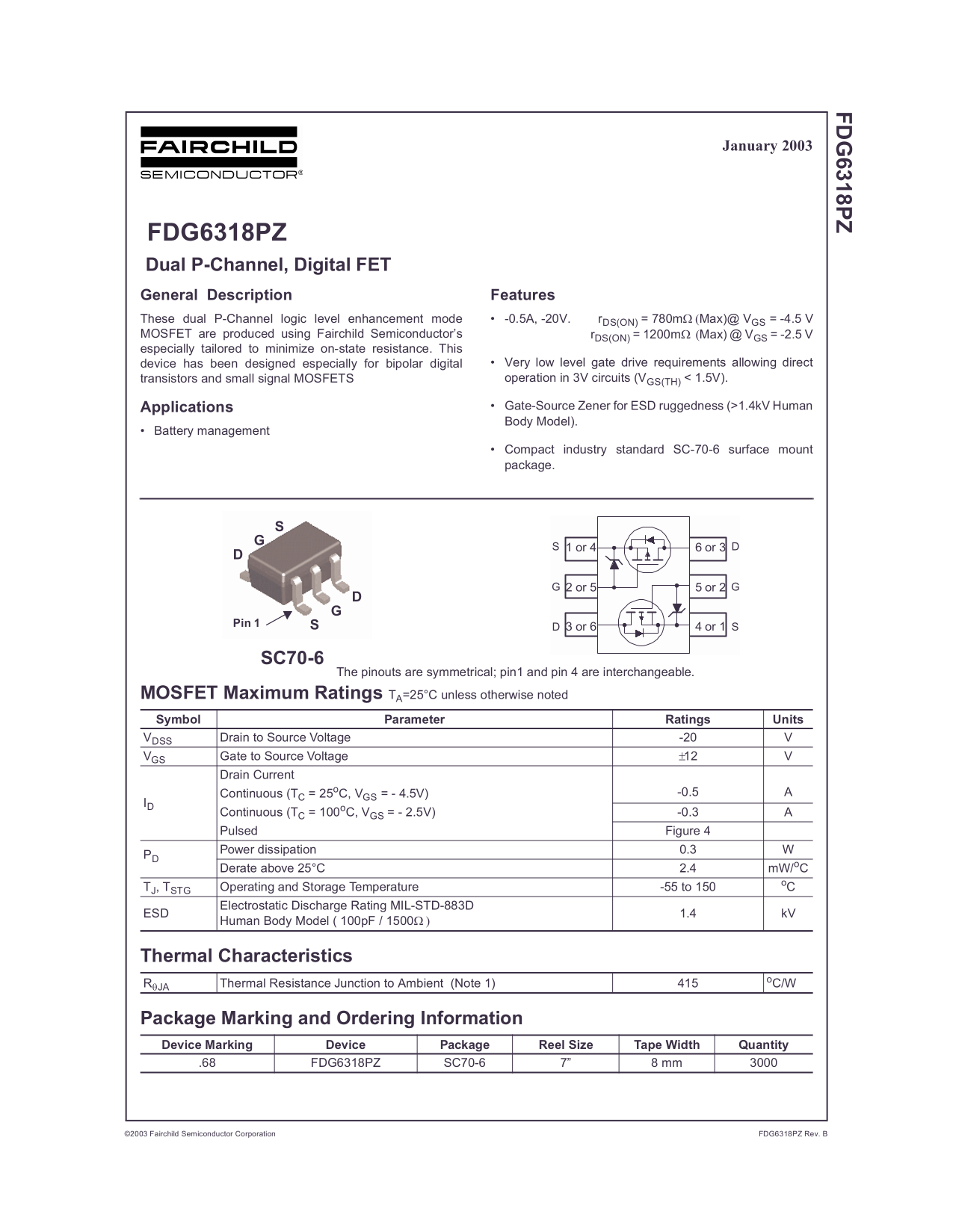
Page 1 Text Content
January
FDG6318PZ Dual P-Channel, Digital FET General Description Features These dual P-Channel logic level enhancement mode -0.5A, -20V. r DS(ON) = 780mΩ (Max)@ VGS = -4.5 V MOSFET are produced using Fairchild Semiconductor’s r DS(ON) = 1200mΩ (Max) @ VGS = -2.5 V especially tailored to minimize on-state resistance. This
device has been designed especially for bipolar digital Very low level gate drive requirements allowing direct transistors and small signal MOSFETS operation in 3V circuits (VGS(TH) < 1.5V).
Applications Gate-Source Zener for ESD ruggedness (>1.4k V Human Body Model).
Battery management
Compact industry standard SC-70-6 surface mount package.
or or
or or
or or
SC70-6
The pinouts are symmetrical; pin1 and pin 4 are interchangeable.
MOSFET Maximum Ratings TA=25°C unless otherwise noted Symbol Parameter Ratings Units VDSS Drain to Source Voltage -20
VGS Gate to Source Voltage ±12 Drain Current
-0.5 AContinuous (TC = 25o C, VGS = - 4.5V)
Continuous (TC = 100o C, VGS = - 2.5V) -0.3 Pulsed Figure 4 Power dissipation 0.3
Derate above 25°C 2.4 m W/o C
TJ, TSTG Operating and Storage Temperature -55 to 150 Electrostatic Discharge Rating MIL-STD-883D
ESD 1.4 k V
Human Body Model ( 100p F / 1500Ω )
Thermal Characteristics
RθJA Thermal Resistance Junction to Ambient (Note 1)
Package Marking and Ordering Information Device Marking Device Package Reel Size Tape Width Quantity
.68 FDG6318PZ SC70-6 7” 8 mm
Fairchild Semiconductor Corporation FDG6318PZ Rev. B
Page Summary Contents For Fairchild FDG6318PZ Dual P-Channel, Digital FET Data Sheet
Manual Details
| Brand | Fairchild |
|---|---|
| Pages | 9 |
| File Size | 217.72 KB |
| Published | July 06, 2026 |
Enter the captcha to get the download link:

Frequently Asked Questions
What type of circuits is this MOSFET designed for?
It has been designed especially for bipolar digital transistors and small signal MOSFETs operation in 3V circuits (V < 1.5V).
Can the component be used as a critical part in life support equipment?
No, Fairchild's products are not authorized for use as critical components in life support devices without express written approval.
What is the Electrostatic Discharge rating of this device?
The ESD rating meets MIL-STD-883D standards at 1.4 kV Human Body Model.
Are there limitations regarding pin arrangement?
No, the pinouts are symmetrical; pin 1 and pin 4 are interchangeable.