Fairchild FDC6401N User Manual
Summary
This dual N-Channel MOSFET is engineered for DC/DC converters, synchronous switching, and power management. Optimized for high efficiency, it features low gate charge, low on-resistance, and fast switching capabilities. Ideal for battery protection and high-power applications.
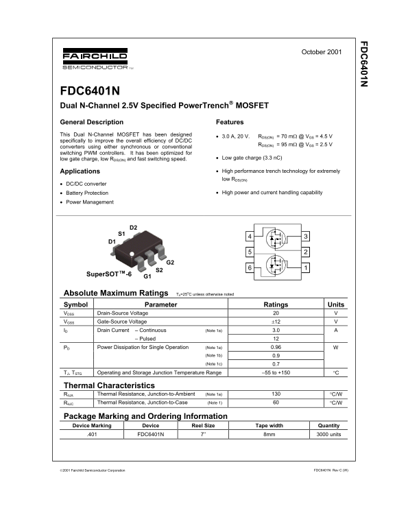
Page 1 Text Content
FD 6401N
October 2001
FDC6401N Dual N-Channel 2.5V Specified Power Trench MOSFET General Description Features This Dual N-Channel MOSFET has been designed
• 3.0 A, 20 V. RDS(ON) = 70 mΩ @ VGS = 4.5 V
specifically to improve the overall efficiency of DC/DC
RDS(ON) = 95 mΩ @ VGS = 2.5 V
converters using either synchronous or conventional switching PWM controllers. It has been optimized for
low gate charge, low RDS(ON) and fast switching speed. • Low gate charge (3.3 n C)
Applications • High performance trench technology for extremely low RDS(ON)
• DC/DC converter
• Battery Protection • High power and current handling capability
• Power Management
Super SOT -6TM
Absolute Maximum Ratings TA=25o C unless otherwise noted Symbol Parameter Ratings Units VDSS Drain-Source Voltage VGSS Gate-Source Voltage ±12 ID Drain Current – Continuous (Note 1a) 3.0
– Pulsed
PD Power Dissipation for Single Operation (Note 1a) 0.96
(Note 1b) 0.9 (Note 1c) 0.7
TJ, TSTG Operating and Storage Junction Temperature Range –55 to +150 °C
Thermal Characteristics
RθJA Thermal Resistance, Junction-to-Ambient (Note 1a) °C/W RθJC Thermal Resistance, Junction-to-Case (Note 1) °C/W
Package Marking and Ordering Information Device Marking Device Reel Size Tape width Quantity
.401 FDC6401N 7’’ 8mm 3000 units
2001 Fairchild Semiconductor Corporation FDC6401N Rev C (W)
Page Summary Contents For Fairchild FDC6401N User Manual
Manual Details
| Brand | Fairchild |
|---|---|
| Pages | 5 |
| File Size | 76.34 KB |
| Published | June 15, 2026 |
Enter the captcha to get the download link:

Frequently Asked Questions
What are the typical applications of FDC6401N?
DC/DC converters, battery protection, and power management.
What is the maximum continuous drain current?
3.0 A when mounted on a minimum pad of 2 oz copper.
What is the on-resistance at 2.5V gate voltage?
95 mΩ typical at VGS=2.5V and ID=2.5A.
What package is FDC6401N available in?
SuperSOT-6 package, supplied in 3000-unit reels.