Fairchild FAN5902 User Manual
Summary
This datasheet documents the Fairchild FAN5902, an 800mA synchronous buck converter designed for powering 3G RF power amplifiers. Features include 92% efficiency, 2.7V to 5.5V input range, dynamic output voltage adjustment from 0.4V to 3.4V, and 6MHz PWM operation enabling 470nH inductor use. Includes integrated bypass FET and thermal shutdown. Targeted at mobile handset designers seeking to improve RFPA efficiency and extend talk time.
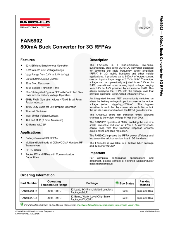
Page 1 Text Content
FA 5902 — 800m uck C onverter for 3G FPA
May 2009
FAN5902 800m A Buck Converter for 3G RFPAs
Features Description
92% Efficient Synchronous Operation The FAN5902 is a high-efficiency, low-noise, synchronous, step-down DC-to-DC converter designed
2.7V to 5.5V Input Voltage Range
for powering the radio frequency power amplifiers (RFPA) in 3G mobile handsets and other mobile
VOUT Range from 0.4V to 3.4V (or VIN)
applications. It provides up to 800m A of output current
Up to 800m A Output Current over an input voltage range of 2.7V to 5.5V. The output
voltage can be dynamically adjusted from 0.4V up to
20µs Step Response
3.4V, proportional to an analog input voltage ranging
30µs Bypass Transition Time from 0.2V to 1.7V provided by an external DAC. This
allows supplying the RFPA with the voltage level that
50mΩ Integrated Bypass FET with Controlled Slew
provides optimum Power Added Efficiency (PAE).
Rate for Low Battery Voltage Operation
An integrated bypass FET automatically switches on
6MHz PWM Operation Allows 470n H Small Form
when the battery voltage drops too close to the output
Factor Inductor
voltage (when VOUT=VBAT-250m V). The bypass
100% Duty Cycle for Low Dropout Operation transition is controlled by a slew rate controller to limit
the inrush current and reduce the RFPA gain deviation.
Thermal Shutdown
The FAN5902 offers fast transition times, allowing
Input Under-Voltage Lockout
changes to the output voltage in less than 20µs.
12-Lead MLP (0.8mm Maximum)
The FAN5902 operates at 6MHz, enabling the use of a
12-Bump WLCSP small, low-value inductor of 470n H. A current-mode
control loop with fast transient response ensures excellent line and load regulation.
Applications
The FAN5902 improves the RFPA power efficiency and
Battery-Powered 3G RFPAs increases the talk/connection time in 3G handsets. Multiband/Multimode WCDMA/CDMA Handset RF The FAN5902 is available in a 12-lead MLP package Transceivers and 12-bump WLCSP. RF PC Cards
Important
Pocket PC and PDAs with Communication Capabilities
For complete performance specifications and datasheet, please contact a Fairchild Semiconductor sales representative.
Ordering Information
Packing
Part Number Operating
Temperature Range Package Eco Status Method
FAN5902MPX -40 to +85°C 12-Lead, 3x3.5mm, Molded Leadless
Package (MLP) Ro HS Tape and Reel
FAN5902UCX -40 to +85°C 12-Bump, Wafer-Level Chip-Scale
Package (WLCSP) Ro HS Tape and Reel
For Fairchild’s definition of Eco Status, please visit: http://www.fairchildsemi.com/company/green/rohs_green.html.
© 2009 Fairchild Semiconductor Corporation www.fairchildsemi.com FAN5902 • Rev. 1.0.2.short
Page Summary Contents For Fairchild FAN5902 User Manual
Manual Details
| Brand | Fairchild |
|---|---|
| Pages | 8 |
| File Size | 391.73 KB |
| Published | June 17, 2026 |
Enter the captcha to get the download link:

Frequently Asked Questions
What is the output voltage range of the FAN5902?
The output voltage (VOUT) can be adjusted from 0.4V up to 3.4V (or up to VIN).
What is the purpose of the integrated bypass FET?
It switches on automatically to supply power directly from the battery when the battery voltage drops too close to the output voltage (VOUT = VBAT - 250mV) to maintain operation.
What package options are available for the FAN5902?
It is available in a 12-lead MLP package and a 12-bump WLCSP.