Toshiba TC7SZ00F, TC7SZ00FU User's Guide
Summary
This professional manual details the reliable integration of the TC7SZ00F/FU, a high-speed, super low-power CMOS 2-Input NAND Gate IC. Designed for advanced digital circuit applications, this component features robust operation across voltages from 1.8V to 5.5V and exceptional output current capabilities. The guide provides critical technical specifications, including detailed electrical characteristics (voltage levels, leakage currents), absolute maximum ratings, comprehensive operational timing parameters, and package dimensions. It is essential reference material for electronics engineers designing reliable, high-performance CMOS logic systems.
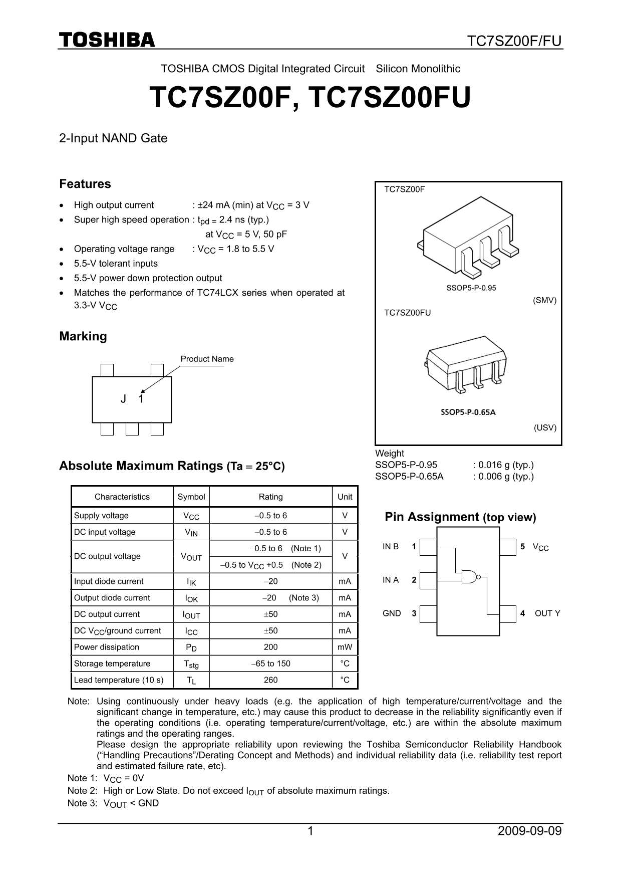
Page 1 Text Content
TC7SZ00F/FU
TOSHIBA CMOS Digital Integrated Circuit Silicon Monolithic
TC7SZ00F, TC7SZ00FU 2-Input NAND Gate
Features
TC7SZ00F
• High output current : ±24 m A (min) at VCC = 3 V • Super high speed operation : tpd = 2.4 ns (typ.)
at VCC = 5 V, 50 p F
• Operating voltage range : VCC = 1.8 to 5.5 V • 5.5-V tolerant inputs • 5.5-V power down protection output • Matches the performance of TC74LCX series when operated at
(SMV)
3.3-V VCC
TC7SZ00FU
Marking
Product Name
(USV)
Weight Absolute Maximum Ratings (Ta = 25°C) SSOP5-P-0.95 : 0.016 g (typ.) SSOP5-P-0.65A : 0.006 g (typ.)
Characteristics Symbol Rating Unit
Supply voltage VCC −0.5 to 6 V Pin Assignment (top view) DC input voltage VIN −0.5 to 6 V
−0.5 to 6 (Note 1) IN B 1 5 VCC
DC output voltage VOUT
−0.5 to VCC +0.5 (Note 2)
Input diode current IIK −20 m A IN A 2
Output diode current IOK −20 (Note 3) m A
DC output current IOUT ±50 m A GND 3 4 OUT Y
DC VCC/ground current ICC ±50 m A
Power dissipation PD 200 m W
Storage temperature Tstg −65 to 150 °C
Lead temperature (10 s) TL 260 °C
Note: Using continuously under heavy loads (e.g. the application of high temperature/current/voltage and the significant change in temperature, etc.) may cause this product to decrease in the reliability significantly even if the operating conditions (i.e. operating temperature/current/voltage, etc.) are within the absolute maximum ratings and the operating ranges. Please design the appropriate reliability upon reviewing the Toshiba Semiconductor Reliability Handbook (“Handling Precautions”/Derating Concept and Methods) and individual reliability data (i.e. reliability test report and estimated failure rate, etc). Note 1: VCC = 0V Note 2: High or Low State. Do not exceed IOUT of absolute maximum ratings. Note 3: VOUT < GND
Page Summary Contents For Toshiba TC7SZ00F, TC7SZ00FU User's Guide
Manual Details
| Brand | Toshiba |
|---|---|
| Pages | 7 |
| File Size | 168.10 KB |
| Published | July 16, 2026 |
Enter the captcha to get the download link:
