Texas Instruments - TLV5618AM-5962 Data Converter User's Manual
Summary
The TLV5618AM is a highly reliable dual 12-bit Digital-to-Analog Converter (DAC) designed for advanced embedded systems. Featuring a flexible 3-wire serial interface compatible with major DSPs, this low-power device provides scalable output voltage accuracy and programmable settling time. Built for extreme environments, it operates on single supply while maintaining reliability across a wide temperature range (-55°C to 125°C). This manual guides engineers through its specifications, ensuring optimal performance in demanding industrial or military applications requiring precise power control.
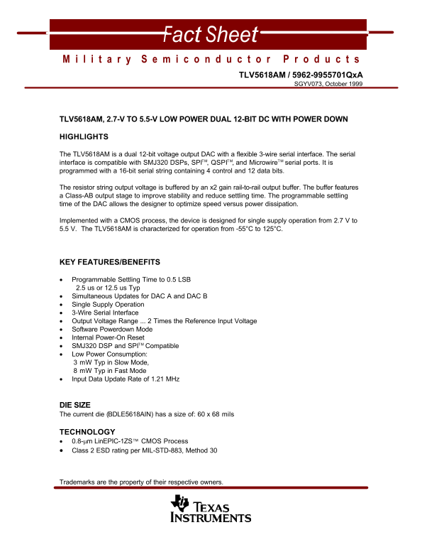
Page 1 Text Content
Fact Sheet Fact Sheet
TLV5618AM / 5962-9955701Qx A SGYV073, October 1999
TLV5618AM, 2.7-V TO 5.5-V LOW POWER DUAL 12-BIT DC WITH POWER DOWN
HIGHLIGHTS
The TLV5618AM is a dual 12-bit voltage output DAC with a flexible 3-wire serial interface. The serial interface is compatible with SMJ320 DSPs, SPITM, QSPITM, and Microwire TM serial ports. It is programmed with a 16-bit serial string containing 4 control and 12 data bits.
The resistor string output voltage is buffered by an x2 gain rail-to-rail output buffer. The buffer features a Class-AB output stage to improve stability and reduce settling time. The programmable settling time of the DAC allows the designer to optimize speed versus power dissipation.
Implemented with a CMOS process, the device is designed for single supply operation from 2.7 V to 5.5 V. The TLV5618AM is characterized for operation from -55°C to 125°C.
KEY FEATURES/BENEFITS
• Programmable Settling Time to 0.5 LSB 2.5 us or 12.5 us Typ • Simultaneous Updates for DAC A and DAC B • Single Supply Operation • 3-Wire Serial Interface • Output Voltage Range ... 2 Times the Reference Input Voltage • Software Powerdown Mode • Internal Power-On Reset • SMJ320 DSP and SPITM Compatible • Low Power Consumption: 3 m W Typ in Slow Mode, 8 m W Typ in Fast Mode • Input Data Update Rate of 1.21 MHz
DIE SIZE The current die (BDLE5618AIN) has a size of: 60 x 68 mils
TECHNOLOGY • 0.8-µm Lin EPIC-1ZS CMOS Process • Class 2 ESD rating per MIL-STD-883, Method 30
Trademarks are the property of their respective owners.
Page Summary Contents For Texas Instruments - TLV5618AM-5962 Data Converter User's Manual
Manual Details
| Brand | Texas Instruments |
|---|---|
| Pages | 3 |
| File Size | 24.72 KB |
| Published | May 28, 2026 |
Enter the captcha to get the download link:

Frequently Asked Questions
What serial interfaces does the TLV5618AM support?
It is compatible with SMJ320 DSPs, SPI, QSPI, and Microwire serial ports.
What is the operating voltage range for single supply operation?
The device operates from 2.7 V to 5.5 V.
What is the guaranteed temperature range for this DAC?
It is characterized for operation from -55°C to 125°C.
How can I optimize power consumption while maintaining performance?
The device features a "Slow Mode" consumption of only 3 mW typ, or you can use Powerdown Mode.