Texas Instruments - THS1206M-5962-9957701NXD Data Converter Owner's Manual and User Guide
Summary
This high-performance Analog-to-Digital Converter (ADC) is designed for specialized applications needing robust signal processing at extreme temperatures. Featuring 12-bit resolution and a 6 MSPS sampling rate, it supports simultaneous acquisition from up to four channels while maintaining low power consumption. Ideal for engineers developing systems in radar, sonar, advanced imaging, and high-speed communications, this component provides reliable data handling across the full military temperature range (–55°C to 125°C).
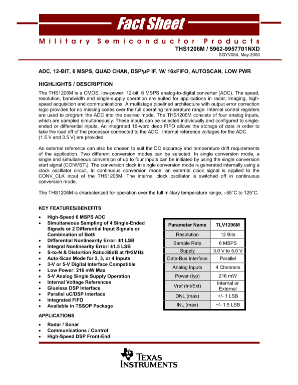
Page 1 Text Content
Fact Sheet
THS1206M / 5962-9957701NXD
SGYV084, May 2000
ADC, 12-BIT, 6 MSPS, QUAD CHAN, DSP/µP IF, W/ 16x FIFO, AUTOSCAN, LOW PWR
HIGHLIGHTS / DESCRIPTION The THS1206M is a CMOS, low-power, 12-bit, 6 MSPS analog-to-digital converter (ADC). The speed, resolution, bandwidth and single-supply operation are suited for applications in radar, imaging, high- speed acquisition and communications. A multistage pipelined architecture with output error correction logic provides for no missing codes over the full operating temperature range. Internal control registers are used to program the ADC into the desired mode. The THS1206M consists of four analog inputs, which are sampled simultaneously. These inputs can be selected individually and configured to single- ended or differential inputs. An integrated 16-word deep FIFO allows the storage of data in order to take the load off of the processor connected to the ADC. Internal reference voltages for the ADC (1.5 V and 3.5 V) are provided.
An external reference can also be chosen to suit the DC accuracy and temperature drift requirements of the application. Two different conversion modes can be selected. In single conversion mode, a single and simultaneous conversion of up to four inputs can be initiated by using the single conversion start signal (CONVST\). The conversion clock in single conversion mode is generated internally using a clock oscillator circuit. In continuous conversion mode, an external clock signal is applied to the CONV_CLK input of the THS1206M. The internal clock oscillator is switched off in continuous conversion mode.
The THS1206M is characterized for operation over the full military temperature range, –55°C to 125°C.
KEY FEATURES/BENEFITS
• High-Speed 6 MSPS ADC • Simultaneous Sampling of 4 Single-Ended
Parameter Name TLV1206M
Signals or 2 Differential Input Signals or
Combination of Both Resolution 12 Bits
• Differential Nonlinearity Error: ±1 LSB
Sample Rate 6 MSPS
• Integral Nonlinearity Error: ±1.5 LSB
Supply 3.0 V to 5.0 V
• S-to-N & Distortion Ratio:68d B at f I=2MHz • Auto-Scan Mode for 2, 3, or 4 Inputs Data-Bus Interface Parallel • 3-V or 5-V Digital Interface Compatible
Analog Inputs 4 Channels
• Low Power: 216 m W Max
• 5-V Analog Single Supply Operation Power (typ) 216 m W
• Internal Voltage References Internal or
Vref (Int/Ext)
• Glueless DSP Interface External • Parallel u C/DSP Interface
DNL (max) +/- 1 LSB
• Integrated FIFO
INL (max) +/- 1.5 LSB
• Available in TSSOP Package
APPLICATIONS
• Radar / Sonar • Communications / Control • High-Speed DSP Front-End
Page Summary Contents For Texas Instruments - THS1206M-5962-9957701NXD Data Converter Owner's Manual and User Guide
Manual Details
| Brand | Texas Instruments |
|---|---|
| Pages | 3 |
| File Size | 106.68 KB |
| Published | May 29, 2026 |
Enter the captcha to get the download link:

Frequently Asked Questions
Does the unit support both single and continuous data acquisition modes?
Yes. It supports single conversion mode using CONVST, or continuous conversion mode by applying an external clock signal to CONV_CLK.
What is the required operational temperature range for this ADC?
The THS1206M is characterized for operation over the full military temperature range: –55°C to 125°C.
Can I use external voltage references or must I rely on internal ones?
You can choose between internal (1.5 V and 3.5 V) or an external reference voltage source based on your application's accuracy needs.
How many channels can be sampled simultaneously using the THS1206M?
It samples up to four analog inputs simultaneously. These can be configured as individual single-ended or differential inputs.