Texas Instruments CD74HC374, CD74HCT374, CD74HC574, CD74HCT574 Owner's Manual and User Guide
Summary
Discover high-performance logic with these Octal D-Type Flip-Flops, engineered for reliable, high-speed data capture in mixed CMOS applications. This comprehensive technical manual serves as an essential datasheet resource, providing engineers and circuit designers with detailed electrical specifications, absolute maximum ratings, temperature ranges, functional diagrams, and pinouts across multiple hardware variations (HC and HCT). Use this guide to accurately integrate stable, robust logic solutions into your critical digital systems.
Page 1 Text Content
CD74HC374, CD74HCT374, CD74HC574, CD74HCT574
Data sheet acquired from Harris Semiconductor SCHS183 High Speed CMOS Logic Octal D-Type Flip-Flop,
February 1998 Three-State Positive-Edge Triggered
Features Description Buffered Inputs The Harris CD74HC374, CD74HCT374, CD74HC574 and
CD74HCT574 are Octal D-Type Flip-Flops with Three-State
[ /Title Common Three-State Output Enable Control
Outputs and the capability to drive LSTTL loads. The eight (CD74 Three-State Outputs edge-triggered flip-flops enter data into their registers on the LOW to HIGH transition of clock (CP). The Output Enable
HC374
Bus Line Driving Capability
(OE) controls the three-state outputs and is independent of Typical Propagation Delay (Clock to Q) = 15ns at the register operation. When Output Enable (OE) is HIGH the
CD74 outputs will be in the high impedance state. The and
VCC = 5V, CL = 15p F, TA = 25o C
HCT37 are identical in function and differ only in their pinout
Fanout (Over Temperature Range)
arrangements.
Standard Outputs . . . . . . . . . . . . . . . 10 LSTTL Loads
Bus Driver Outputs . . . . . . . . . . . . . 15 LSTTL Loads Ordering Information
HC574
Wide Operating Temperature Range . . . -55o C to 125o C PKG.
PART NUMBER TEMP. RANGE (o C) PACKAGE NO.
Balanced Propagation Delay and Transition Times
CD74HC374E -55 to 125 20 Ld PDIP E20.3
HCT57 Significant Power Reduction Compared to LSTTL
CD74HCT374E -55 to 125 20 Ld PDIP E20.3
Logic ICs
CD74HCT574E -55 to 125 20 Ld PDIP E20.3
HC Types CD74HC574E -55 to 125 20 Ld PDIP E20.3 2V to 6V Operation CD74HC574M -55 to 125 20 Ld SOIC M20.3 High Noise Immunity: NIL = 30%, NIH = 30% of VCC CD74HC374M -55 to 125 20 Ld SOIC M20.3 at VCC = 5V
CD74HCT374M -55 to 125 20 Ld SOIC M20.3 HCT Types CD74HCT574M -55 to 125 20 Ld SOIC M20.3 4.5V to 5.5V Operation NOTES: Direct LSTTL Input Logic Compatibility, 1. When ordering, use the entire part number. Add the suffix to VIL= 0.8V (Max), VIH = 2V (Min) obtain the variant in the tape and reel. CMOS Input Compatibility, Il 1µA at VOL, VOH 2. Wafer and die for this part number is available which meets all electrical specifications. Please contact your local sales office or Harris customer service for ordering information.
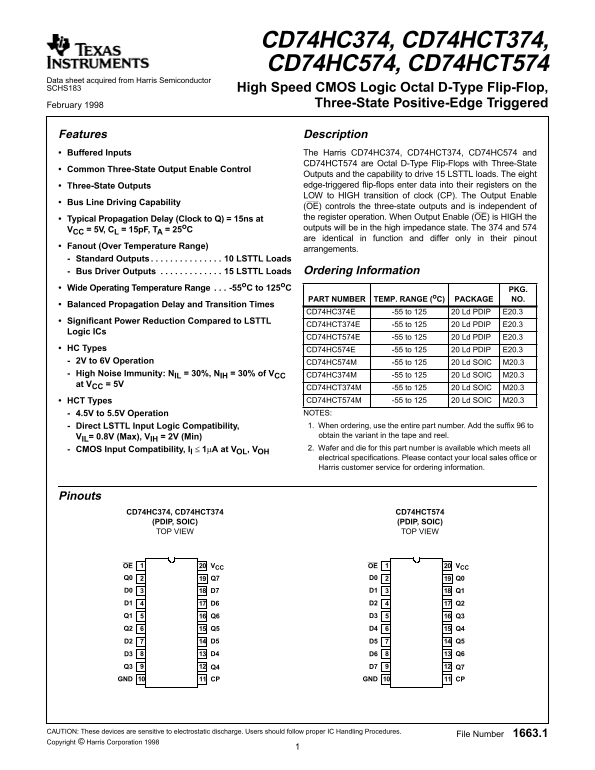
Pinouts
CD74HC374, CD74HCT374 CD74HCT574 (PDIP, SOIC) (PDIP, SOIC) TOP VIEW TOP VIEW
1OE VCC 1OE VCC Q0 Q7 D0 Q0 D0 D7 D1 Q1 D1 D6 D2 Q2 Q1 Q6 D3 Q3 Q2 Q5 D4 Q4
Q3 Q4 D7 Q7 GND CP GND CP
CAUTION: These devices are sensitive to electrostatic discharge. Users should follow proper IC Handling Procedures.
File Number 1663.1
Copyright © Harris Corporation 1998
Page Summary Contents For Texas Instruments CD74HC374, CD74HCT374, CD74HC574, CD74HCT574 Owner's Manual and User Guide
Manual Details
| Brand | Texas Instruments |
|---|---|
| Pages | 9 |
| File Size | 52.10 KB |
| Published | May 28, 2026 |
Enter the captcha to get the download link:

Frequently Asked Questions
What is the typical propagation delay?
The typical propagation delay (Clock to Q) for the CD74 series is 15ns at standard conditions (V=5V, C=15pF, T=25°C).
Are all four chip versions identical in function?
Yes, the CD74 and CD74HCT families are identical in function; they only differ in their pinout arrangements (PDIP or SOIC).
What is the maximum operating temperature range?
The devices support a Wide Operating Temperature Range from -55°C to 125°C.
Does Output Enable (OE) affect register operation?
No, the bus line driving capability (OE) controls the three-state outputs and is independent of the internal register operation.