Texas Instruments SN54ACT573, SN74ACT573 Owner's Manual
Summary
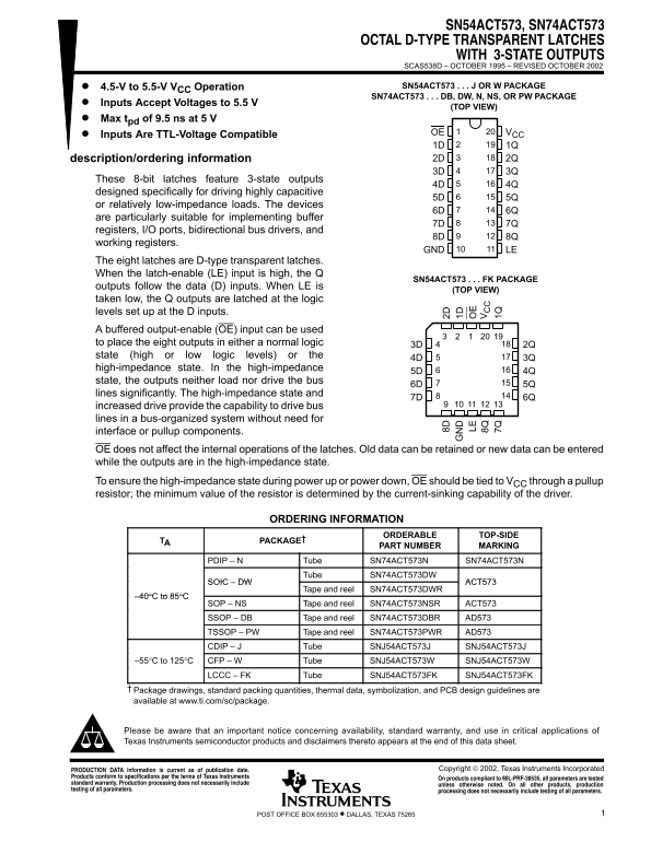
This datasheet from Texas Instruments documents the SN54ACT573 and SN74ACT573 octal D-type transparent latches with 3-state outputs, operating from a 4.5 V to 5.5 V supply with a maximum propagation delay of 9.5 ns at 5 V. The eight latches feature a latch-enable input that makes Q outputs transparent to D inputs when high and latches data on the falling edge, plus a buffered output-enable input for placing outputs in a high-impedance state suitable for bus-organized systems. The document includ
Page 1 Text Content
SN54ACT573, SN74ACT573
OCTAL D-TYPE TRANSPARENT LATCHES
WITH 3-STATE OUTPUTS SCAS538D – OCTOBER 1995 – REVISED OCTOBER 2002
4.5-V to 5.5-V VCC Operation SN54ACT573 J OR W PACKAGE SN74ACT573 DB, DW, N, NS, OR PW PACKAGE
Inputs Accept Voltages to 5.5 V
(TOP VIEW)
Max tpd of 9.5 ns at 5 V
Inputs Are TTL-Voltage Compatible OE VCC
1D 1Q description/ordering information 2D 2Q 3D 3Q
These 8-bit latches feature 3-state outputs
designed specifically for driving highly capacitive
or relatively low-impedance loads. The devices
are particularly suitable for implementing buffer
registers, I/O ports, bidirectional bus drivers, and
working registers.
GND LE
The eight latches are D-type transparent latches. When the latch-enable (LE) input is high, the Q
SN54ACT573 FK PACKAGE
outputs follow the data (D) inputs. When LE is
(TOP VIEW)
taken low, the Q outputs are latched at the logic levels set up at the D inputs. A buffered output-enable (OE) input can be used to place the eight outputs in either a normal logic 3D 2Q state (high or low logic levels) or the
high-impedance state. In the high-impedance
state, the outputs neither load nor drive the bus
lines significantly. The high-impedance state and
increased drive provide the capability to drive bus lines in a bus-organized system without need for interface or pullup components.
OE does not affect the internal operations of the latches. Old data can be retained or new data can be entered
while the outputs are in the high-impedance state. 1D
To ensure the high-impedance state during power up or power down, OE should be tied to VCC through a pullup
resistor; the minimum value of the resistor is determined by the current-sinking capability of the driver.
ORDERING INFORMATION
ORDERABLE TOP-SIDE
TA PACKAGE†
PART NUMBER MARKING
PDIP – N Tube SN74ACT573N SN74ACT573N
Tube SN74ACT573DW
SOIC DW ACT573
Tape and reel SN74ACT573DWR
40°C to 85°C
SOP – NS Tape and reel SN74ACT573NSR ACT573 SSOP – DB Tape and reel SN74ACT573DBR AD573 TSSOP – PW Tape and reel SN74ACT573PWR AD573 CDIP – J Tube SNJ54ACT573J SNJ54ACT573J
–55°C to 125°C CFP – W Tube SNJ54ACT573W SNJ54ACT573W
LCCC – FK Tube SNJ54ACT573FK SNJ54ACT573FK
Package drawings, standard packing quantities, thermal data, symbolization, and PCB design guidelines are available at www.ti.com/sc/package.
Please be aware that an important notice concerning availability, standard warranty, and use in critical applications of Texas Instruments semiconductor products and disclaimers thereto appears at the end of this data sheet.
Copyright 2002, Texas Instruments Incorporated PRODUCTION DATA information is current as of publication date.
Products conform to specifications per the terms of Texas Instruments On products compliant to MIL-PRF-38535, all parameters are tested standard warranty. Production processing does not necessarily include unless otherwise noted. On all other products, production testing of all parameters. processing does not necessarily include testing of all parameters.
1POST OFFICE BOX 655303 • DALLAS, TEXAS 75265
Page Summary Contents For Texas Instruments SN54ACT573, SN74ACT573 Owner's Manual
Manual Details
| Brand | Texas Instruments |
|---|---|
| Pages | 16 |
| File Size | 530.24 KB |
| Published | June 20, 2026 |
Enter the captcha to get the download link:

Frequently Asked Questions
When are the Q outputs following the D inputs?
The Q outputs follow the data (D) inputs when the latch-enable (LE) input is high.
What state do I use to prevent lines from loading or driving the bus?
Use the high-impedance state, achieved by setting OE high, which prevents the outputs from significantly loading or driving the lines.
How must I connect OE for proper power up/down retention?
To ensure the high-impedance state during power up or power down, OE should be tied to V through a pullup resistor.