# A B C D E F G H I J K L M N O P Q R S T U V W X Y Z

Texas Instruments ADS1602 16-Bit, 2.5 MSPS Analog-to-Digital Converter User's Manual and Data Sheet

Summary

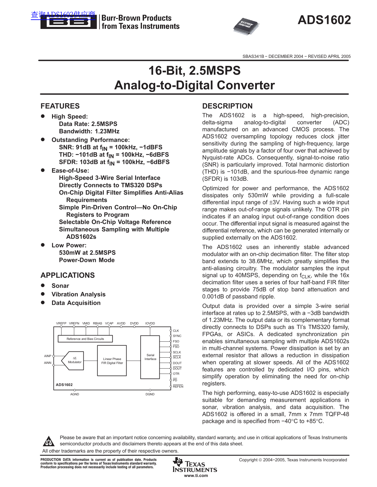
The ADS1602 is a high-performance, 16-Bit delta-sigma Analog-to-Digital Converter (ADC) boasting a fast 2.5MSPS data rate and exceptional precision. This manual provides comprehensive technical specifications, detailing superior performance metrics like high SNR and THD, along with low power dissipation features. It is designed for demanding data acquisition applications, making it ideal for use in sonar systems, vibration analysis, and other complex measurement setups integrated with DSPs.
📄 Preview PAGE OF 26

Page 1 Text Content

查询ADS1602供应商

ADS1602

SBAS341B − DECEMBER 2004 − REVISED APRIL 2005

16-Bit, 2.5MSPS Analog-to-Digital Converter

FEATURES DESCRIPTION

High Speed: The ADS1602 is a high-speed, high-precision, delta-sigma analog-to-digital converter (ADC)

Data Rate: 2.5MSPS

manufactured on an advanced CMOS process. The

Bandwidth: 1.23MHz

ADS1602 oversampling topology reduces clock jitter

Outstanding Performance:

sensitivity during the sampling of high-frequency, large

SNR: 91d B at f IN = 100k Hz, −1d BFS

amplitude signals by a factor of four over that achieved by

THD: −101d B at f IN = 100k Hz, −6d BFS

Nyquist-rate ADCs. Consequently, signal-to-noise ratio

SFDR: 103d B at f IN = 100k Hz, −6d BFS

(SNR) is particularly improved. Total harmonic distortion

Ease-of-Use: (THD) is −101d B, and the spurious-free dynamic range High-Speed 3-Wire Serial Interface (SFDR) is 103d B. Directly Connects to TMS320 DSPs

Optimized for power and performance, the ADS1602

On-Chip Digital Filter Simplifies Anti-Alias

dissipates only 530m W while providing a full-scale

Requirements

differential input range of ±3V. Having such a wide input

Simple Pin-Driven Control—No On-Chip

range makes out-of-range signals unlikely. The OTR pin

Registers to Program

indicates if an analog input out-of-range condition does

Selectable On-Chip Voltage Reference

occur. The differential input signal is measured against the

Simultaneous Sampling with Multiple differential reference, which can be generated internally or ADS1602s supplied externally on the ADS1602. Low Power:

The ADS1602 uses an inherently stable advanced

530m W at 2.5MSPS modulator with an on-chip decimation filter. The filter stop Power-Down Mode band extends to 38.6MHz, which greatly simplifies the

anti-aliasing circuitry. The modulator samples the input APPLICATIONS signal up to 40MSPS, depending on f CLK, while the 16x decimation filter uses a series of four half-band FIR filter

Sonar

stages to provide 75d B of stop band attenuation and

Vibration Analysis

0.001d B of passband ripple.

Data Acquisition

Output data is provided over a simple 3-wire serial interface at rates up to 2.5MSPS, with a −3d B bandwidth of 1.23MHz. The output data or its complementary format

VREFP VREFN RBIASVMID VCAP AVDD DVDD IOVDD

directly connects to DSPs such as TI’s TMS320 family,

SYNC FPGAs, or ASICs. A dedicated synchronization pin

Reference and Bias Circuits

FSO enables simultaneous sampling with multiple ADS1602s FSO

in multi-channel systems. Power dissipation is set by an

AINP Serial external resistor that allows a reduction in dissipation

∆Σ SCLK

Phase Interface Linear

AINN Modulator FIR Digital Filter DOUT when operating at slower speeds. All of the ADS1602

features are controlled by dedicated I/O pins, which

simplify operation by eliminating the need for on-chip

registers.

REFENADS1602

DGNDAGND The high performing, easy-to-use ADS1602 is especially suitable for demanding measurement applications in sonar, vibration analysis, and data acquisition. The ADS1602 is offered in a small, 7mm x 7mm TQFP-48 package and is specified from −40°C to +85°C.

Please be aware that an important notice concerning availability, standard warranty, and use in critical applications of Texas Instruments semiconductor products and disclaimers thereto appears at the end of this data sheet. All other trademarks are the property of their respective owners.

Copyright  2004−2005, Texas Instruments Incorporated

www.ti.com

Page Summary Contents For Texas Instruments ADS1602 16-Bit, 2.5 MSPS Analog-to-Digital Converter User's Manual and Data Sheet

Page 1 查询ADS1602供应商 ADS1602 SBAS341B − DECEMBER 2004 − REVISED APRIL 2005 16-Bit, 2.5MSPS Analog-to-Digital Converter FEATURES DESCRIPTION High Speed: The ADS1602 is a high-speed, high-precision, delta-sigma...
Page 2 www.ti.com SBAS341B − DECEMBER 2004 − REVISED APRIL 2005 PACKAGE/ORDERING INFORMATION This integrated circuit can be damaged by ESD. Texas Instruments recommends that all integrated circuits be For th...
Page 3 www.ti.com SBAS341B − DECEMBER 2004 − REVISED APRIL 2005 ELECTRICAL CHARACTERISTICS All specifications at TA = −40°C to +85°C, AVDD = 5V, DVDD = IOVDD = 3V, f CLK = 40MHz, External VREF = +3V, VCM = +...
Page 4 www.ti.com SBAS341B − DECEMBER 2004 − REVISED APRIL 2005 ELECTRICAL CHARACTERISTICS (continued) All specifications at TA = −40°C to +85°C, AVDD = 5V, DVDD = IOVDD = 3V, f CLK = 40MHz, External VREF = ...
Page 5 www.ti.com SBAS341B − DECEMBER 2004 − REVISED APRIL 2005 ELECTRICAL CHARACTERISTICS (continued) All specifications at TA = −40°C to +85°C, AVDD = 5V, DVDD = IOVDD = 3V, f CLK = 40MHz, External VREF = ...
Page 6 www.ti.com SBAS341B − DECEMBER 2004 − REVISED APRIL 2005 DEFINITIONS Absolute Input Voltage Intermodulation Distortion (IMD) Absolute input voltage, given in volts, is the voltage of each IMD, given i...
Page 7 www.ti.com SBAS341B − DECEMBER 2004 − REVISED APRIL 2005 PIN ASSIGNMENTS AGND DGND AVDD NC AGND DVDD AINN DGND AINP FSO AGND FSO TQFP PACKAGE ADS1602 AVDD DOUT (TOP VIEW) RBIAS DOUT AGND SCLK LU ID AV...
Page 8 www.ti.com SBAS341B − DECEMBER 2004 − REVISED APRIL 2005 TIMING DIAGRAMS t STL SYNC t SYPW Figure 1. Initialization Timing TIMING REQUIREMENTS For TA = −40°C to +85°C, DVDD = 2.7V to 3.6V, IOVDD = 2.7...
Page 9 www.ti.com SBAS341B − DECEMBER 2004 − REVISED APRIL 2005 TYPICAL CHARACTERISTICS pl itu (d pl itu de (d lit ud (d All specifications at TA = 25°C, AVDD = 5V, DVDD = IOVDD = 3V, f CLK = 40MHz, External...
Page 10 www.ti.com SBAS341B − DECEMBER 2004 − REVISED APRIL 2005 pl itu de (d pl itu de (d lit ud (d TYPICAL CHARACTERISTICS (continued) All specifications at TA = 25°C, AVDD = 5V, DVDD = IOVDD = 3V, f CLK = ...
Page 11 www.ti.com SBAS341B − DECEMBER 2004 − REVISED APRIL 2005 IG L− IS IO IG L− IS AT IO IG L− IS AT IO TYPICAL CHARACTERISTICS (continued) TA IC IS IO TA IC IS IO TA IC IS IO IO IC (d IO IC (d IO IC (d Al...
Page 12 www.ti.com SBAS341B − DECEMBER 2004 − REVISED APRIL 2005 (d (d TYPICAL CHARACTERISTICS (continued) All specifications at TA = 25°C, AVDD = 5V, DVDD = IOVDD = 3V, f CLK = 40MHz, External VREF = +3V, VC...
Page 13 www.ti.com SBAS341B − DECEMBER 2004 − REVISED APRIL 2005 TYPICAL CHARACTERISTICS (continued) cc rr en ce (d All specifications at TA = 25°C, AVDD = 5V, DVDD = IOVDD = 3V, f CLK = 40MHz, External VREF ...
Page 14 www.ti.com SBAS341B − DECEMBER 2004 − REVISED APRIL 2005 (d up pl ur re nt (m TYPICAL CHARACTERISTICS (continued) All specifications at TA = 25°C, AVDD = 5V, DVDD = IOVDD = 3V, f CLK = 40MHz, External...
Page 15 www.ti.com SBAS341B − DECEMBER 2004 − REVISED APRIL 2005 OVERVIEW digital output code of 7FFFh. Likewise, the most negative measurable differential input is –VREF, which produces the The ADS1602 is a ...
Page 16 www.ti.com SBAS341B − DECEMBER 2004 − REVISED APRIL 2005 INPUT CIRCUITRY external capacitors, between the inputs and from each input to AGND, improve linearity and should be placed as The ADS1602 uses...
Page 17 www.ti.com SBAS341B − DECEMBER 2004 − REVISED APRIL 2005 REFERENCE INPUTS (VREFN, VREFP, VMID) of providing both a dc and a transient current. Figure 44 shows a simplified diagram of the internal circ...
Page 18 www.ti.com SBAS341B − DECEMBER 2004 − REVISED APRIL 2005 CLOCK INPUT (CLK) DATA FORMAT The ADS1602 requires an external clock signal to be The 16-bit output data is in binary two’s complement applied ...
Page 19 www.ti.com SBAS341B − DECEMBER 2004 − REVISED APRIL 2005 INITIALIZING THE ADS1602 STEP RESPONSE After the power supplies have stabilized, you must Figure 47 plots the normalized step response for an i...
Page 20 www.ti.com ag ni tu de (d ag itu de (d SBAS341B − DECEMBER 2004 − REVISED APRIL 2005 FREQUENCY RESPONSE The linear phase FIR digital filter sets the overall frequency f CLK 40MHz response. Figure 48 s...
Page 21 www.ti.com SBAS341B − DECEMBER 2004 − REVISED APRIL 2005 ANALOG POWER DISSIPATION Table 3. Recommended RBIAS Resistor Values for Different CLK Frequencies An external resistor connected between the RB...
Page 22 www.ti.com SBAS341B − DECEMBER 2004 − REVISED APRIL 2005 POWER SUPPLIES ground, as shown in Figure 53. Each main supply bus Three supplies are used on the ADS1602: analog (AVDD), should also be bypass...
Page 23 www.ti.com SBAS341B − DECEMBER 2004 − REVISED APRIL 2005 LAYOUT ISSUES AND COMPONENT SELECTION The Mc BSP provides a host of functions including: The ADS1602 is a very high-speed, high-resolution data...
Page 24 PACKAGE OPTION ADDENDUM www.ti.com 19-Apr-2005 PACKAGING INFORMATION Orderable Device Status Package Package Pins Package Eco Plan Lead/Ball Finish MSL Peak Temp Type Drawing Qty ADS1602IPFBR ACTIVE T...
Page 25 MECHANICAL DATA MTQF019A – JANUARY 1995 – REVISED JANUARY 1998 PFB (S-PQFP-G48) PLASTIC QUAD FLATPACK 0,13 NOM 5,50 TYP 7,20 SQ Gage Plane 6,80 9,20 SQ 8,80 0,25 0,05 MIN Seating Plane 0,45 1,20 MAX N...
Page 26 IMPORTANT NOTICE Texas Instruments Incorporated and its subsidiaries (TI) reserve the right to make corrections, modifications, enhancements, improvements, and other changes to its products and servic...