# A B C D E F G H I J K L M N O P Q R S T U V W X Y Z

Texas Instruments TL1451A-Q1 Data Sheet

Summary

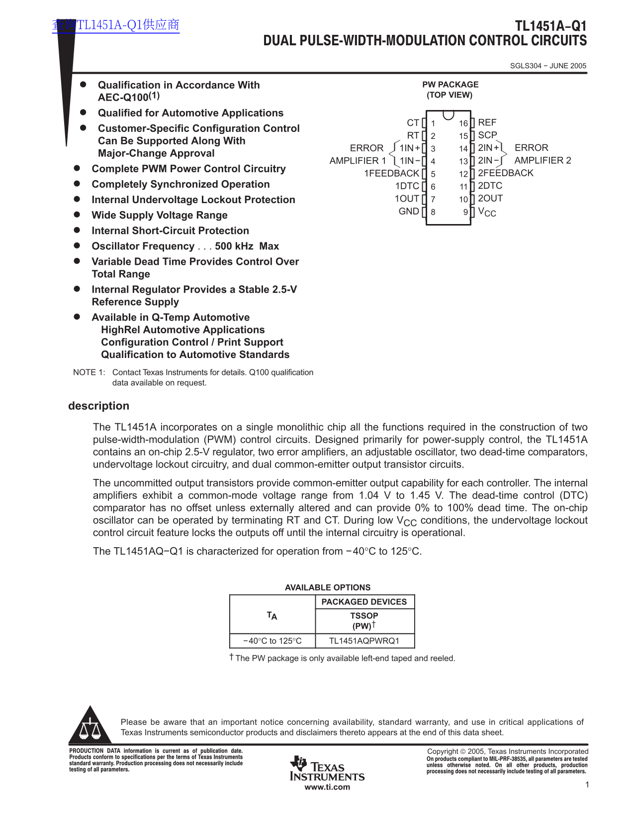
The TL1451A is a specialized monolithic chip designed for robust power-supply control, integrating two complete Pulse-Width Modulation (PWM) circuits into one unit. This manual details its technical capabilities, including on-chip 2.5V regulation, error amplification, and adjustable dead-time comparators. Featuring undervoltage lockout and wide operating voltage ranges, the TL1451AQ-Q1 is engineered for mission-critical applications, making it an ideal choice for automotive systems that require high reliability and AEC-Q100 qualification (-40°C to 125°C).
📄 Preview PAGE OF 22

Page 1 Text Content

查询TL1451A-Q1供应商

SGLS304 − JUNE 2005

Qualification in Accordance With PW PACKAGE (TOP VIEW)

AEC-Q100(1) Qualified for Automotive Applications

CT REF

Customer-Specific Configuration Control

RT SCP

Can Be Supported Along With

ERROR 1IN+ 2IN+ ERROR

Major-Change Approval

AMPLIFIER 1 1IN− 2IN− AMPLIFIER 2

Complete PWM Power Control Circuitry

1FEEDBACK 2FEEDBACK

Completely Synchronized Operation 1DTC 2DTC

Internal Undervoltage Lockout Protection 1OUT 2OUT GND VCC

Wide Supply Voltage Range Internal Short-Circuit Protection Oscillator Frequency 500 k Hz Max Variable Dead Time Provides Control Over Total Range Internal Regulator Provides a Stable 2.5-V Reference Supply Available in Q-Temp Automotive High Rel Automotive Applications Configuration Control / Print Support Qualification to Automotive Standards NOTE 1: Contact Texas Instruments for details. Q100 qualification data available on request.

description The TL1451A incorporates on a single monolithic chip all the functions required in the construction of two pulse-width-modulation (PWM) control circuits. Designed primarily for power-supply control, the TL1451A contains an on-chip 2.5-V regulator, two error amplifiers, an adjustable oscillator, two dead-time comparators, undervoltage lockout circuitry, and dual common-emitter output transistor circuits. The uncommitted output transistors provide common-emitter output capability for each controller. The internal amplifiers exhibit a common-mode voltage range from 1.04 V to 1.45 V. The dead-time control (DTC) comparator has no offset unless externally altered and can provide 0% to 100% dead time. The on-chip oscillator can be operated by terminating RT and CT. During low VCC conditions, the undervoltage lockout control circuit feature locks the outputs off until the internal circuitry is operational. The TL1451AQ−Q1 is characterized for operation from −40°C to 125°C.

AVAILABLE OPTIONS

PACKAGED DEVICES

TA TSSOP

−40°C to 125°C TL1451AQPWRQ1

The PW package is only available left-end taped and reeled.

Please be aware that an important notice concerning availability, standard warranty, and use in critical applications of Texas Instruments semiconductor products and disclaimers thereto appears at the end of this data sheet.

1www.ti.com

Page Summary Contents For Texas Instruments TL1451A-Q1 Data Sheet

Page 1 查询TL1451A-Q1供应商 SGLS304 − JUNE 2005 Qualification in Accordance With PW PACKAGE (TOP VIEW) AEC-Q100(1) Qualified for Automotive Applications CT REF Customer-Specific Configuration Control RT SCP Can B...
Page 2 SGLS304 − JUNE 2005 functional block diagram VCC RT CT 2 DTC ERROR IN+ 2 OUTPUT AMPLIFIER 2 2 FEEDBACK PWM Oscillator 1/2 Vref 1 FEEDBACK Reference 12 kΩ Voltage 170 kΩ UVLO ERROR AMPLIFIER 1 1 OUTPUT...
Page 3 SGLS304 − JUNE 2005 absolute maximum ratings over operating free-air temperature range† Supply voltage, VCC 51 V. . . . . . . . . . . . . . . . . . . . . . . . . . . . . . . . . . . . . . . . . . . . ...
Page 4 SGLS304 − JUNE 2005 electrical characteristics over recommended operating free-air temperature range, VCC = 6 V, f = 200 k Hz (unless otherwise noted) reference section TL1451AQ PARAMETER TEST CONDITI...
Page 5 SGLS304 − JUNE 2005 short-circuit protection control section TL1451AQ PARAMETER TEST CONDITIONS UNIT MIN TYP† MAX TA = 25°C Input threshold voltage (SCP) TA = 125°C m V TA = MIN Standby voltage (SCP) ...
Page 6 SGLS304 − JUNE 2005 error-amplifier section TL1451AQ PARAMETER TEST CONDITIONS UNIT MIN TYP† MAX TA = 25°C ±7 Input offset voltage VO (FEEDBACK) = 1.25 V TA = 125°C ±10 m V TA = MIN ±12 TA = 25°C ±100...
Page 7 SGLS304 − JUNE 2005 total device TL1451AQ PARAMETER TEST CONDITIONS UNIT MIN TYP† MAX Standby supply current Off-state 1.3 1.8 m A Average supply current RT = 10 kΩ 1.7 2.4 m A All typical values are ...
Page 8 Tr ia le av ef rm in lt ag fo sc ri an le sc ill at re en cy SGLS304 − JUNE 2005 TYPICAL CHARACTERISTICS TRIANGLE OSCILLATOR FREQUENCY OSCILLATOR FREQUENCY VARIATION vs vs TIMING RESISTANCE FREE-AIR T...
Page 9 SGLS304 − JUNE 2005 av re ef er en ce tp Vo lt ag ar ia ti re ef er en ce tp Vo lt ag (r ef (r ef TYPICAL CHARACTERISTICS REFERENCE OUTPUT VOLTAGE VARIATION REFERENCE OUTPUT VOLTAGE VARIATION vs vs FR...
Page 10 tp lle ct Vo lt ag SGLS304 − JUNE 2005 TYPICAL CHARACTERISTICS UNDERVOLTAGE LOCKOUT HYSTERESIS CHARACTERISTICS UNDERVOLTAGE LOCKOUT CHARACTERISTIC 3.5 TA = 25°C TA = 85°C TA = −20°C Threshold Voltage ...
Page 11 SGLS304 − JUNE 2005 TYPICAL CHARACTERISTICS PROTECTION ENABLE TIME PROTECTION ENABLE CAPACITANCE tp ro te ct io ab le im CPE − Protection Enable Capacitance − µF SCP Vref 170 kΩ Vref Vref Short-circui...
Page 12 rr ax im tp Vo lt ag in SGLS304 − JUNE 2005 TYPICAL CHARACTERISTICS ERROR AMP MAXIMUM OUTPUT VOLTAGE SWING OPEN-LOOP VOLTAGE AMPLIFICATION vs vs FREQUENCY FREQUENCY 2.25 VCC = 5 V VCC = 5 V TA = 25°C ...
Page 13 SGLS304 − JUNE 2005 lo se -L ai TYPICAL CHARACTERISTICS CLOSED-LOOP GAIN AND PHASE SHIFT vs FREQUENCY VCC = 5 V CX: 47 p F Rref = 150 Ω 470 p F Cref = 470 p F 4700 p F TA = 25°C Phase Shift (Right Sca...
Page 14 lo se -L ai SGLS304 − JUNE 2005 TYPICAL CHARACTERISTICS CLOSED-LOOP GAIN AND PHASE SHIFT vs FREQUENCY VCC = 5 V CX: 47 p F Rref = 15 Ω 470 p F Cref = 470 p F 4700 p F TA = 25°C Phase Shift (Right Scal...
Page 15 SGLS304 − JUNE 2005 lo se -L ai TYPICAL CHARACTERISTICS CLOSED-LOOP GAIN AND PHASE SHIFT vs FREQUENCY VCC = 5 V CX: 47 p F Rref = 15 Ω 470 p F Cref = 470 p F 4700 p F TA = 25°C Phase Shift (Right Scal...
Page 16 lo se -L ai SGLS304 − JUNE 2005 TYPICAL CHARACTERISTICS CLOSED-LOOP GAIN AND PHASE SHIFT vs FREQUENCY VCC = 5 V Cref = 470 p F TA = 25°C 0° Closed-Loop Gain −10° Phase Shift (Left Scale) −20° (Right S...
Page 17 SGLS304 − JUNE 2005 ax im TYPICAL CHARACTERISTICS tp Vo lt ag in OUTPUT SINK CURRENT COLLECTOR OUTPUT SATURATION VOLTAGE TA = −20°C TA = 25°C TA = 85°C tp in rr en VCC = 3.6 V Collector Output Saturat...
Page 18 IC ly rr en tp Tr an si st “O ty yc le SGLS304 − JUNE 2005 TYPICAL CHARACTERISTICS OUTPUT TRANSISTOR ON DUTY CYCLE STANDBY CURRENT DEAD-TIME INPUT VOLTAGE SUPPLY VOLTAGE VCC = 3.6 V TA = 25°C RT = 10k...
Page 19 SGLS304 − JUNE 2005 APPLICATION INFORMATION Step-Up C2 Output TL1451A Step-Down C4 Output NOTE A: Values for R1 through R7, C1 through C4, and L1 and L2 depend upon individual application. Figure 28. ...
Page 20 PACKAGE OPTION ADDENDUM www.ti.com 27-Feb-2006 PACKAGING INFORMATION Orderable Device Status Package Package Pins Package Eco Plan Lead/Ball Finish MSL Peak Temp Type Drawing Qty TL1451AQPWRQ1 ACTIVE ...
Page 21 MECHANICAL DATA MTSS001C – JANUARY 1995 – REVISED FEBRUARY 1999 PW (R-PDSO-G**) PLASTIC SMALL-OUTLINE PACKAGE 14 PINS SHOWN 0,15 NOM Gage Plane Seating Plane 1,20 MAX 0,10 PINS ** DIM A MAX 3,10 5,10 ...
Page 22 IMPORTANT NOTICE Texas Instruments Incorporated and its subsidiaries (TI) reserve the right to make corrections, modifications, enhancements, improvements, and other changes to its products and servic...

Manual Details

Brand Texas Instruments
Pages 22
File Size 319.43 KB
Published July 15, 2026
1 views

Enter the captcha to get the download link:

captcha

Frequently Asked Questions

What range of dead time can I set for the DTC comparator?

The DTC comparator supports an adjustable dead time ranging from 0% to 100%.

Does the device provide protection during low voltage conditions?

Yes, the Undervoltage Lockout (UVLO) circuit locks the outputs off until the internal circuitry is fully operational.

What is the operating temperature range for the TL1451AQ-Q1 variant?

It is characterized for operation from -40°C to 125°C and is qualified for automotive applications.