Texas Instruments SN74LVC1G04 Single Inverter Gate Data Sheet
Summary
This single inverter gate is an essential logic component engineered for digital circuits requiring robust performance across a wide operating range of 1.65V to 5.5V. Featuring low power consumption and high ESD protection, the model supports partial-power-down mode via NanoStar™ technology. This resource provides comprehensive technical specifications, ordering details for various packages (including lead-free options), electrical characteristics, and usage guidelines. It is ideal for electronic engineers and hardware designers integrating reliable, space-efficient logic into advanced digital systems and embedded applications.
Page 1 Text Content
查询SN74LVC1G04供应商
SN74LVC1G04
SINGLE INVERTER GATE
www.ti.com
SCES214S–APRIL 1999–REVISED OCTOBER
FEATURES
Available in the Texas Instruments Ioff Supports Partial-Power-Down Mode
Nano Star™ and Nano Free™ Packages Operation
Supports 5-V VCC Operation Latch-Up Performance Exceeds m A Per
JESD 78, Class II•
Inputs Accept Voltages to 5.5
ESD Protection Exceeds JESD 22•
Max tpd of 3.3 ns at 3.3
2000-V Human-Body Model (A114-A)•
Low Power Consumption, 10-µA Max ICC
200-V Machine Model (A115-A)•
±24-m A Output Drive at 3.3
1000-V Charged-Device Model (C101)
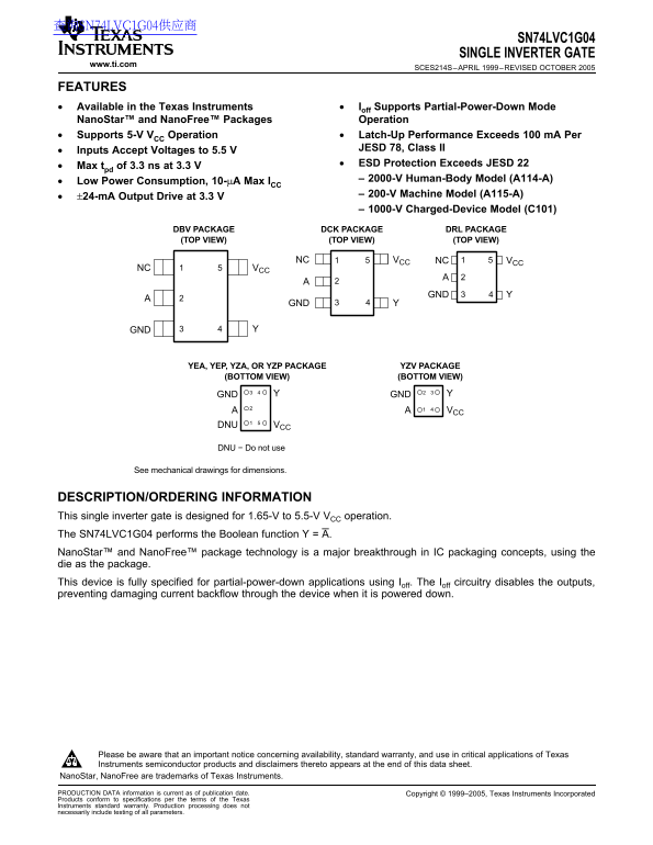
DBV PACKAGE DCK PACKAGE DRL PACKAGE (TOP VIEW) (TOP VIEW) (TOP VIEW)
51NC VCC 51NC VCC
51NC VCC
YEA, YEP, YZA, OR YZP PACKAGE YZV PACKAGE
(BOTTOM VIEW) (BOTTOM VIEW)
GND GND
DNU VCC
DNU − Do not use
See mechanical drawings for dimensions.
DESCRIPTION/ORDERING INFORMATION
This single inverter gate is designed for 1.65-V to 5.5-V VCC operation.
The SN74LVC1G04 performs the Boolean function A.
Nano Star™ and Nano Free™ package technology is major breakthrough in IC packaging concepts, using the
die as the package.
This device is fully specified for partial-power-down applications using Ioff. The Ioff circuitry disables the outputs,
preventing damaging current backflow through the device when it is powered down.
Please be aware that an important notice concerning availability, standard warranty, and use in critical applications of Texas
Instruments semiconductor products and disclaimers thereto appears at the end of this data sheet.
Nano Star, Nano Free are trademarks of Texas Instruments.
PRODUCTION DATA information is current as of publication date. Copyright 1999–2005, Texas Instruments Incorporated
Products conform to specifications per the terms of the Texas
Instruments standard warranty. Production processing does not
necessarily include testing of all parameters.
Page Summary Contents For Texas Instruments SN74LVC1G04 Single Inverter Gate Data Sheet
Manual Details
| Brand | Texas Instruments |
|---|---|
| Pages | 17 |
| File Size | 442.73 KB |
| Published | June 18, 2026 |
Enter the captcha to get the download link:

Frequently Asked Questions
What is the typical operating voltage range for this inverter gate?
It is designed for operation from 1.65-V to 5.5-V.
Does the SN74LVC1G04 support low power consumption modes?
Yes, it supports partial-power-down applications using auxiliary circuitry (I), which disables outputs and prevents damaging backflow current when powered down.
What is the maximum rated input/output voltage range?
The maximum rating for both input and output voltages is -0.5 V to 6.5 V.
How is the device packaged and what variations are available?
It is available in various packages like NanoStar™, NanoFree™, DBV, DCK, and DRL, with specific orderable parts listed for different surface-mount types.