TEXAS INSTRUMENTS SN54AHCT32, SN74AHCT32 Quadruple 2-Input Positive-NOR Gates Data Sheet
Summary
This comprehensive technical manual details the SN74AHCT32/SN54AHCT32 family of quadruple 2-input Positive-OR gates. These high-reliability logic components perform core Boolean functions in positive logic and are designed to be TTL voltage compatible. The documentation provides detailed functional information, including absolute maximum ratings, robust ESD/Latch-Up specifications, diverse packaging options (e.g., DIP, SOIC, TSSOP), and thermal data across various operating temperature ranges. This guide is essential for electronic engineers and hardware designers requiring accurate integration of reliable OR gate functionality into their circuit boards.
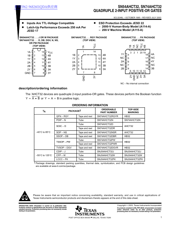
Page 1 Text Content
查询5962-9682601QDA供应商 SN54AHCT32, SN74AHCT32
QUADRUPLE 2-INPUT POSITIVE-OR GATES
SCLS248L – OCTOBER 1995 – REVISED JULY 2003
Inputs Are TTL-Voltage Compatible ESD Protection Exceeds JESD 22
– 2000-V Human-Body Model (A114-A)
Latch-Up Performance Exceeds 250 m A Per
– 200-V Machine Model (A115-A)
JESD 17
SN54AHCT32 J OR W PACKAGE SN74AHCT32 RGY PACKAGE SN54AHCT32 FK PACKAGE SN74AHCT32 D, DB, DGV, N, NS, (TOP VIEW) (TOP VIEW)
OR PW PACKAGE (TOP VIEW)
1A VCC
NC NC
NC NC
2Y 3A GND 3Y
NC – No internal connection 1A
description/ordering information The ’AHCT32 devices are quadruple 2-input positive-OR gates. These devices perform the Boolean function 3Y
or B in positive logic.
ORDERING INFORMATION
ORDERABLE TOP-SIDE
TA PACKAGE†
PART NUMBER MARKING
QFN – RGY Tape and reel SN74AHCT32RGYR HB32 PDIP – N Tube SN74AHCT32N SN74AHCT32N
Tube SN74AHCT32D
SOIC AHCT32
Tape and reel SN74AHCT32DR
–40°C to 85°C SOP – NS Tape and reel SN74AHCT32NSR AHCT32
SSOP – DB Tape and reel SN74AHCT32DBR HB32
Tube SN74AHCT32PW
TSSOP PW HB32 –
Tape and reel SN74AHCT32PWR 3A
TVSOP – DGV Tape and reel SN74AHCT32DGVR HB32 CDIP – J Tube SNJ54AHCT32J SNJ54AHCT32J
–55°C to 125°C CFP – W Tube SNJ54AHCT32W SNJ54AHCT32W
LCCC – FK Tube SNJ54AHCT32FK SNJ54AHCT32FK
Package drawings, standard packing quantities, thermal data, symbolization, and PCB design guidelines are available at www.ti.com/sc/package.
Please be aware that an important notice concerning availability, standard warranty, and use in critical applications of Texas Instruments semiconductor products and disclaimers thereto appears at the end of this data sheet.
PRODUCTION DATA information is current as of publication date. Copyright 2003, Texas Instruments Incorporated
Products conform to specifications per the terms of Texas Instruments On products compliant to MIL-PRF-38535, all parameters are tested standard warranty. Production processing does not necessarily include unless otherwise noted. On all other products, production testing of all parameters. processing does not necessarily include testing of all parameters.
1POST OFFICE BOX 655303 • DALLAS, TEXAS 75265
Page Summary Contents For TEXAS INSTRUMENTS SN54AHCT32, SN74AHCT32 Quadruple 2-Input Positive-NOR Gates Data Sheet
Manual Details
| Brand | Texas Instruments |
|---|---|
| Pages | 19 |
| File Size | 598.99 KB |
| Published | June 06, 2026 |
Enter the captcha to get the download link:

Frequently Asked Questions
What Boolean function do these gates perform?
They are quadruple 2-input positive-OR gates, performing Y = A OR B in positive logic.
What is the specified operating voltage range for VCC?
The supply voltage range (VCC) must be between –0.5 V and 7 V.
What are the limits for storage temperature?<
The device has a wide storage temperature range of –65°C to 150°C.
What is the maximum continuous output current?
The continuous output current, Io, is rated at ±25 mA.