Texas Instruments - CD54HC259, CD74HC259, CD54HCT259, CD74HCT259 High-Speed CMOS Logic 8-Bit Addressable Latch
Summary
These datasheets detail the versatile CD/CD74 series of 8-Bit Addressable Latches. Designed for engineers implementing high-speed digital logic, these low-power CMOS ICs provide reliable data storage across four flexible operating modes—including Memory and Demultiplexer. The documentation covers full electrical specifications, operational principles, and compatibility details, offering robust performance in demanding thermal ranges from -55°C to 125°C for advanced circuit design applications.
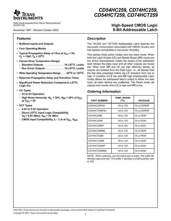
Page 1 Text Content
CD54HC259, CD74HC259, CD54HCT259, CD74HCT259
Data sheet acquired from Harris Semiconductor SCHS173C High-Speed CMOS Logic November 1997 - Revised October 2003 8-Bit Addressable Latch
Features Description Buffered Inputs and Outputs The ’HC259 and ’HCT259 Addressable Latch features the
low-power consumption associated with CMOS circuitry and
[ /Title Four Operating Modes
has speeds comparable to low-power Schottky.
(CD74 Typical Propagation Delay of 15ns at VCC = 5V,
This latches three active modes and one reset mode. When
HC259 CL = 15p F, TA = 25o C
both the Latch Enable (LE) and Master Reset (MR) inputs are Fanout (Over Temperature Range) low (8-line Demultiplexer mode) the output of the addressed latch follows the Data input and all other outputs are forced
CD74 Standard Outputs . . . . . . . . . . . . . . . 10 LSTTL Loads
low. When both MR and LE are high (Memory Mode), all
HCT25 Bus Driver Outputs . . . . . . . . . . . . . 15 LSTTL Loads
outputs are isolated from the Data input, i.e., all latches hold
9) Wide Operating Temperature Range . . . -55o C to 125o C the last data presented before the LE transition from low to
/Sub- high. condition of LE low and MR high (Addressable Latch
Balanced Propagation Delay and Transition Times
mode) allows the addressed latch’s output to follow the data
Significant Power Reduction Compared to LSTTL input; all other latches are unaffected. The Reset mode (all
(High
Logic ICs outputs low) results when LE is high and MR is low.
Speed
HC Types
CMOS Ordering Information
2V to 6V Operation
Logic
High Noise Immunity: NIL = 30%, NIH = 30% of VCC TEMP. RANGE
8-Bit
at VCC = 5V PART NUMBER (o C) PACKAGE
Addres
HCT Types CD54HC259F3A -55 to 125 16 Ld CERDIP
sable
4.5V to 5.5V Operation
CD54HCT259F3A -55 to 125 16 Ld CERDIP
Latch)
Direct LSTTL Input Logic Compatibility,
VIL= 0.8V (Max), VIH = 2V (Min) CD74HC259E -55 to 125 16 Ld PDIP
CMOS Input Compatibility, Il 1µA at VOL, VOH
CD74HC259M -55 to 125 16 Ld SOIC
CD74HC259MT -55 to 125 16 Ld SOIC
CD74HC259M96 -55 to 125 16 Ld SOIC
CD74HCT259E -55 to 125 16 Ld PDIP
CD74HCT259M -55 to 125 16 Ld SOIC
CD74HCT259MT -55 to 125 16 Ld SOIC
CD74HCT259M96 -55 to 125 16 Ld SOIC
NOTE: When ordering, use the entire part number. The suffix denotes tape and reel. The suffix denotes small-quantity reel of 250.
CAUTION: These devices are sensitive to electrostatic discharge. Users should follow proper IC Handling Procedures. Copyright © 2003, Texas Instruments Incorporated
Page Summary Contents For Texas Instruments - CD54HC259, CD74HC259, CD54HCT259, CD74HCT259 High-Speed CMOS Logic 8-Bit Addressable Latch
Manual Details
| Brand | Texas Instruments |
|---|---|
| Pages | 14 |
| File Size | 276.47 KB |
| Published | June 21, 2026 |
Enter the captcha to get the download link:

Frequently Asked Questions
What is the operating temperature range for these addressable latches?
They feature a wide operational temperature range of -55°C to 125°C.
How should I determine compatibility between HC and HCT types?
HC types operate from 2V to 6V, while HCT types require a supply voltage of 4.5V to 5.5V.
What must I do regarding handling these devices?
The devices are sensitive to electrostatic discharge (ESD), and users should follow proper IC Handling Procedures.
How does the latch operate in Memory Mode?
In Memory Mode (MR=High, LE=High), the latches hold the last data presented before the Latch Enable transitioned from low to high.