TEXAS INSTRUMENTS - CD54/CD74HCT540/CD54/CD74HC540 High-Speed CMOS Logic Octal Buffer and Line Drivers, Three- State Data Manual / User Guide
Summary
These versatile Octal Buffer and Line Drivers are essential logic integrated circuits designed for high-performance signal buffering and line driving. The manual provides detailed technical specifications for models in the HC and HCT families (e.g., CD74HC540), covering three-state outputs, wide operating temperatures (-55°C to 125°C), and varied voltage compatibility. Ideal for engineers requiring reliable buffering capabilities, these ICs support robust signal management in complex digital systems.
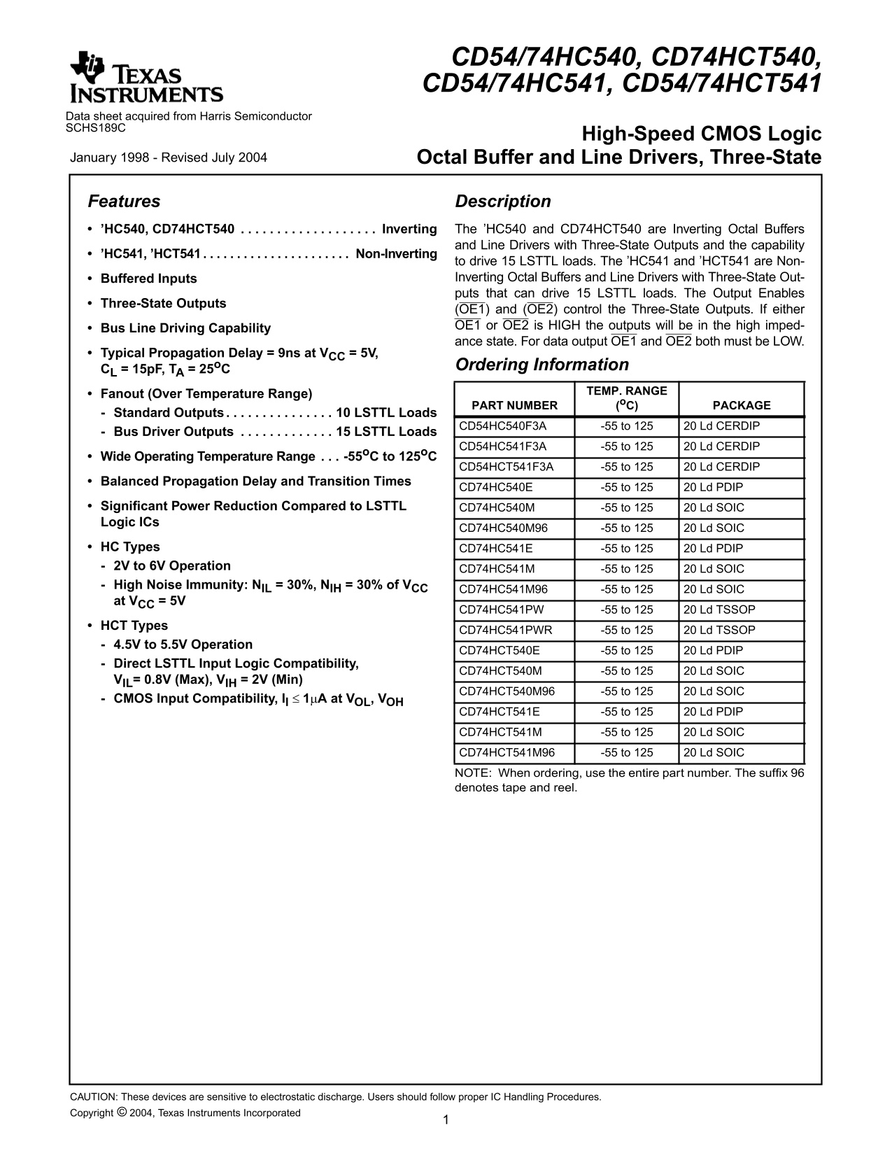
Page 1 Text Content
CD54/74HC540, CD74HCT540, CD54/74HC541, CD54/74HCT541
Data sheet acquired from Harris Semiconductor SCHS189C
High-Speed CMOS Logic
January 1998 - Revised July 2004 Octal Buffer and Line Drivers, Three-State
Features Description ’HC540, CD74HCT540 . . . . . . . . . . . . . . . . . . . Inverting The ’HC540 and CD74HCT540 are Inverting Octal Buffers
and Line Drivers with Three-State Outputs and the capability
[ /Title ’HC541, ’HCT541 . . . . . . . . . . . . . . . . . . . . . . Non-Inverting
to drive LSTTL loads. The ’HC541 and ’HCT541 are Non- (CD74 Buffered Inputs Inverting Octal Buffers and Line Drivers with Three-State Out- puts that can drive LSTTL loads. The Output Enables
HC540
Three-State Outputs
(OE1) and (OE2) control the Three-State Outputs. If either Bus Line Driving Capability OE1 or OE2 is HIGH the outputs will be in the high imped-
CD74 ance state. For data output OE1 and OE2 both must be LOW.
Typical Propagation Delay = 9ns at VCC = 5V,
HCT54
CL = 15p F, TA = 25o C Ordering Information
Fanout (Over Temperature Range) TEMP. RANGE
PART NUMBER (o C) PACKAGE
Standard Outputs . . . . . . . . . . . . . . . 10 LSTTL Loads
HC541
CD54HC540F3A -55 to 125 20 Ld CERDIP
Bus Driver Outputs . . . . . . . . . . . . . 15 LSTTL Loads
CD54HC541F3A -55 to 125 20 Ld CERDIP
Wide Operating Temperature Range . . . -55o C to 125o C
CD54HCT541F3A -55 to 125 20 Ld CERDIP
HCT54 Balanced Propagation Delay and Transition Times
CD74HC540E -55 to 125 20 Ld PDIP
Significant Power Reduction Compared to LSTTL CD74HC540M -55 to 125 20 Ld SOIC Logic ICs
CD74HC540M96 -55 to 125 20 Ld SOIC
HC Types CD74HC541E -55 to 125 20 Ld PDIP 2V to 6V Operation CD74HC541M -55 to 125 20 Ld SOIC High Noise Immunity: NIL = 30%, NIH = 30% of VCC
CD74HC541M96 -55 to 125 20 Ld SOIC
at VCC = 5V
CD74HC541PW -55 to 125 20 Ld TSSOP
HCT Types
CD74HC541PWR -55 to 125 20 Ld TSSOP
4.5V to 5.5V Operation
CD74HCT540E -55 to 125 20 Ld PDIP
Direct LSTTL Input Logic Compatibility,
CD74HCT540M -55 to 125 20 Ld SOIC
VIL= 0.8V (Max), VIH = 2V (Min)
CD74HCT540M96 -55 to 125 20 Ld SOIC
CMOS Input Compatibility, Il 1µA at VOL, VOH
CD74HCT541E -55 to 125 20 Ld PDIP CD74HCT541M -55 to 125 20 Ld SOIC CD74HCT541M96 -55 to 125 20 Ld SOIC NOTE: When ordering, use the entire part number. The suffix denotes tape and reel.
CAUTION: These devices are sensitive to electrostatic discharge. Users should follow proper IC Handling Procedures. Copyright © 2004, Texas Instruments Incorporated
Page Summary Contents For TEXAS INSTRUMENTS - CD54/CD74HCT540/CD54/CD74HC540 High-Speed CMOS Logic Octal Buffer and Line Drivers, Three- State Data Manual / User Guide
Manual Details
| Brand | Texas Instruments |
|---|---|
| Pages | 16 |
| File Size | 321.44 KB |
| Published | June 22, 2026 |
Enter the captcha to get the download link:

Frequently Asked Questions
What condition is required to enable data output via the three-state outputs?
Both Output Enable pins (OE1 and OE2) must be LOW.
Which device type offers direct compatibility with legacy TTL inputs?
The HCT series devices (e.g., CD74HCT540) are designed for this capability.
What is the operating temperature range for these logic chips?
The recommended operational temperature range is from -55°C to 125°C.
Are there specific handling precautions for using these ICs?
Yes, users must follow proper IC Handling Procedures because these devices are sensitive to electrostatic discharge.