Texas Instruments CD54 74HC123, 74HCT123, 74HC423, 74HCT423 High Speed CMOS Logic Dual Retriggerable Monostable Multivibrators with Resets
Summary
These dual monostable multivibrators are essential components for generating reliable, precise electrical pulses within high-speed CMOS logic systems. The accompanying manual details comprehensive specifications for multiple models, covering features like retriggering inputs, differential edge triggering, and controllable resets. It provides critical guidance on performance parameters, including optimizing output pulse width using external resistors ($\text{R}_x$) and capacitors ($\text{C}$), ensuring reliable circuit design across industrial temperature ranges.
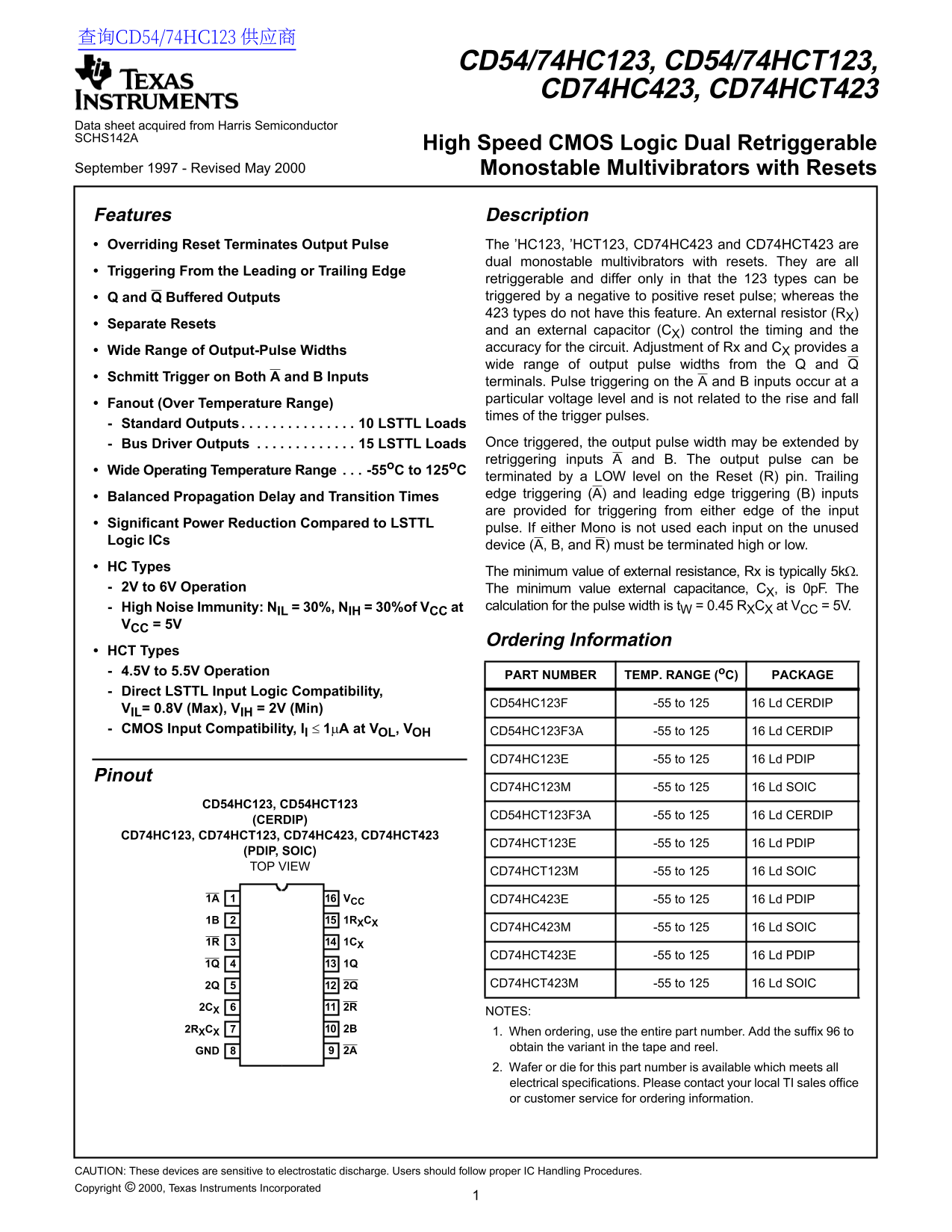
Page 1 Text Content
查询CD54/74HC123 供应商
CD54/74HC123, CD54/74HCT123, CD74HC423, CD74HCT423
Data sheet acquired from Harris Semiconductor SCHS142A
High Speed CMOS Logic Dual Retriggerable
September 1997 - Revised May 2000 Monostable Multivibrators with Resets
Features Description Overriding Reset Terminates Output Pulse The ’HC123, ’HCT123, CD74HC423 and CD74HCT423 are
dual monostable multivibrators with resets. They are all
[ /Title Triggering From the Leading or Trailing Edge
retriggerable and differ only in that the types can be (CD74 Q and Q Buffered Outputs triggered by negative to positive reset pulse; whereas the types do not have this feature. An external resistor (RX)
HC123
Separate Resets
and an external capacitor (CX) control the timing and the Wide Range of Output-Pulse Widths accuracy for the circuit. Adjustment of Rx and CX provides
CD74 wide range of output pulse widths from the and
Schmitt Trigger on Both A and B Inputs
HCT12 terminals. Pulse triggering on the and inputs occur at particular voltage level and is not related to the rise and fall
3, Fanout (Over Temperature Range)
times of the trigger pulses.
CD74 Standard Outputs . . . . . . . . . . . . . . . 10 LSTTL Loads
Bus Driver Outputs . . . . . . . . . . . . . 15 LSTTL Loads Once triggered, the output pulse width may be extended by
HC423
retriggering inputs and B. The output pulse can be
Wide Operating Temperature Range . . . -55o C to 125o C
terminated by LOW level on the Reset (R) pin. Trailing
CD74 edge triggering (A) and leading edge triggering (B) inputs
Balanced Propagation Delay and Transition Times
HCT42 are provided for triggering from either edge of the input
Significant Power Reduction Compared to LSTTL
pulse. If either Mono is not used each input on the unused
Logic ICs
device (A, B, and R) must be terminated high or low.
/Sub-
HC Types
The minimum value of external resistance, Rx is typically 5kΩ.
2V to 6V Operation The minimum value external capacitance, CX, is 0p F. The
(High
High Noise Immunity: NIL 30%, NIH 30%of VCC at calculation for the pulse width is t W = 0.45 RXCX at VCC = 5V.
Speed VCC = 5V
Ordering Information
HCT Types 4.5V to 5.5V Operation
PART NUMBER TEMP. RANGE (o C) PACKAGE
Direct LSTTL Input Logic Compatibility,
CD54HC123F -55 to 125 16 Ld CERDIP
VIL= 0.8V (Max), VIH = 2V (Min) CMOS Input Compatibility, Il 1µA at VOL, VOH CD54HC123F3A -55 to 125 16 Ld CERDIP
CD74HC123E -55 to 125 16 Ld PDIP
Pinout
CD74HC123M -55 to 125 16 Ld SOIC
CD54HC123, CD54HCT123
CD54HCT123F3A -55 to 125 16 Ld CERDIP
(CERDIP)
CD74HC123, CD74HCT123, CD74HC423, CD74HCT423
CD74HCT123E -55 to 125 16 Ld PDIP
(PDIP, SOIC) TOP VIEW
CD74HCT123M -55 to 125 16 Ld SOIC
1A VCC CD74HC423E -55 to 125 16 Ld PDIP 1B 1RXCX
CD74HC423M -55 to 125 16 Ld SOIC
1R 1CX
CD74HCT423E -55 to 125 16 Ld PDIP
2Q 2Q CD74HCT423M -55 to 125 16 Ld SOIC
2CX 2R
NOTES:
2RXCX 2B
1. When ordering, use the entire part number. Add the suffix to 2A obtain the variant in the tape and reel.
2. Wafer or die for this part number is available which meets all electrical specifications. Please contact your local TI sales office or customer service for ordering information.
CAUTION: These devices are sensitive to electrostatic discharge. Users should follow proper IC Handling Procedures. Copyright © 2000, Texas Instruments Incorporated
Page Summary Contents For Texas Instruments CD54 74HC123, 74HCT123, 74HC423, 74HCT423 High Speed CMOS Logic Dual Retriggerable Monostable Multivibrators with Resets
Manual Details
| Brand | Texas Instruments |
|---|---|
| Pages | 8 |
| File Size | 43.53 KB |
| Published | July 15, 2026 |
Enter the captcha to get the download link:

Frequently Asked Questions
What components are required to control the pulse timing?
The circuit requires an external resistor (Rx) and an external capacitor (C) to control the timing of the output pulse width.
What electrical precautions must be taken when handling these ICs?
These devices are sensitive to electrostatic discharge; users must follow proper IC Handling Procedures.
What is the operational voltage supply range for this device?
The DC Supply Voltage, VCC, operates over a range of -0.5V to 7V.
How can these monostable multivibrators be triggered?
They are capable of triggering from both the leading edge (B) and trailing edge (A) inputs, or can utilize an overriding Reset pin.