Texas Instruments CD54HC10, CD74HC10, CD54HCT10, CD74HCT10 High-Speed CMOS Logic Triple 3-Input NAND Gate Owner's Manual
Summary
These high-speed CMOS NAND Gate logic integrated circuits offer reliable, low-power digital switching for complex electronic systems. Designed with compatibility across various logic families (LS, HCT) and a wide operating temperature range (-55°C to 125°C), they are ideal for mission-critical circuit design. This datasheet provides comprehensive technical details, including precise electrical specifications, guaranteed timing parameters, absolute maximum ratings, and recommended implementation guidelines for electronics engineers and hardware architects integrating digital control logic.
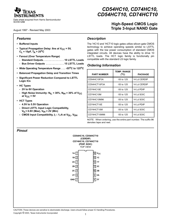
Page 1 Text Content
CD54HC10, CD74HC10, CD54HCT10, CD74HCT10
Data sheet acquired from Harris Semiconductor SCHS128B
High-Speed CMOS Logic Triple 3-Input NAND Gate
August 1997 - Revised May 2003
Features Description
[ /Title
Buffered Inputs The ’HC10 and ’HCT10 logic gates utilize silicon gate CMOS
(CD74
technology to achieve operating speeds similar to LSTTL
HC10, Typical Propagation Delay: 8ns at VCC = 5V,
gates with the low power consumption of standard CMOS
CL = 15p F, TA = 25o C
CD74 integrated circuits. All devices have the ability to drive
HCT10 Fanout (Over Temperature Range) LSTTL loads. The HCT logic family is functionally pin compatible with the standard LS logic family.
Standard Outputs . . . . . . . . . . . . . . . 10 LSTTL Loads /Sub- Bus Driver Outputs . . . . . . . . . . . . . 15 LSTTL Loads
Ordering Information
ject Wide Operating Temperature Range . . . -55o C to 125o C
(High TEMP. RANGE
Balanced Propagation Delay and Transition Times
PART NUMBER (o C) PACKAGE
Speed
Significant Power Reduction Compared to LSTTL
CMOS CD54HC10F3A -55 to 125 14 Ld CERDIP
Logic ICs
Logic
CD54HCT10F3A -55 to 125 14 Ld CERDIP
HC Types
Triple
2V to 6V Operation CD74HC10E -55 to 125 14 Ld PDIP
3-Input
High Noise Immunity: NIL = 30%, NIH = 30% of VCC
CD74HC10M -55 to 125 14 Ld SOIC
NAND at VCC = 5V Gate) CD74HC10M96 -55 to 125 14 Ld SOIC
HCT Types
/Autho
4.5V to 5.5V Operation CD74HCT10E -55 to 125 14 Ld PDIP
Direct LSTTL Input Logic Compatibility,
CD74HCT10M -55 to 125 14 Ld SOIC
/Key- VIL= 0.8V (Max), VIH = 2V (Min)
words CMOS Input Compatibility, Il 1µA at VOL, VOH CD74HCT10M96 -55 to 125 14 Ld SOIC
(High
NOTE: When ordering, use the entire part number. The suffix Speed denotes tape and reel.
CMOS Logic Pinout Triple
CD54HC10, CD54HCT10
3-Input (CERDIP)
CD74HC10, CD74HCT10
(PDIP, SOIC)
Gate,
TOP VIEW
1A VCC
Speed
CMOS 1B 1C Logic 2A 1Y
Triple 2B 3C 3-Input
Gate,
GND 3Y
Harris Semi-
CAUTION: These devices are sensitive to electrostatic discharge. Users should follow proper IC Handling Procedures. Copyright © 2003, Texas Instruments Incorporated
Page Summary Contents For Texas Instruments CD54HC10, CD74HC10, CD54HCT10, CD74HCT10 High-Speed CMOS Logic Triple 3-Input NAND Gate Owner's Manual
Manual Details
| Brand | Texas Instruments |
|---|---|
| Pages | 9 |
| File Size | 137.70 KB |
| Published | May 28, 2026 |
Enter the captcha to get the download link:

Frequently Asked Questions
What are the operating temperature ranges for these logic gates?
The devices support a wide operating temperature range of -55°C to 125°C.
Do the HCT types support different voltage levels than HC types?
Yes, HC types operate between 2V to 6V, while HCT types require a supply voltage range of 4.5V to 5.5V.
How many LSTTL loads can the integrated circuits drive from their standard outputs?
All devices have the ability to drive 10 LSTTL loads.
Is there electrostatic discharge risk when handling these components?
Yes, caution is advised as these devices are sensitive to electrostatic discharge, requiring proper IC Handling Procedures.