Texas Instruments SN54ABT853, SN74ABT853 8-Bit to 9-Bit Parity Bus Transceivers Datasheet Manual
Summary
Enhance data system reliability with these 8-bit to 9-bit parity transceivers (SN54ABT853/SN74ABT853). Designed for critical communication paths, this device automatically generates and checks a parity bit, providing robust error detection during bus transfers. The comprehensive manual serves as an essential guide for electrical engineers and system designers, detailing technical specifications, operational modes, and implementation guidelines needed to build ultra-reliable digital systems requiring integrated data integrity monitoring.
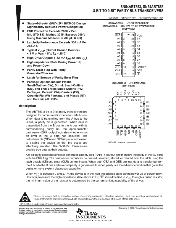
Page 1 Text Content
SN54ABT853, SN74ABT853
8-BIT TO 9-BIT PARITY BUS TRANSCEIVERS SCBS198F – FEBRUARY 1991 – REVISED OCTOBER 1997
State-of-the-Art EPIC-ΙΙB Bi CMOS Design SN54ABT853 JT OR W PACKAGE SN74ABT853 DB, DW, NT, OR PW PACKAGE
Significantly Reduces Power Dissipation
(TOP VIEW)
ESD Protection Exceeds 2000 V Per MIL-STD-883, Method 3015; Exceeds 200 V OEA VCC Using Machine Model (C = 200 p F, R = 0) A1 B1
Latch-Up Performance Exceeds 500 m A Per A2 B2 JESD 17 A3 B3 A4 B4
Typical VOLP (Output Ground Bounce)
< 1 V at VCC = 5 V, TA = 25°C
High-Drive Outputs (–32-m A IOH, 64-m A IOL)
High-Impedance State During Power Up
and Power Down
ERR PARITY
Parity-Error Flag With Parity CLR OEB Generator/Checker GND LE Latch for Storage of Parity-Error Flag Package Options Include Plastic
SN54ABT853 FK PACKAGE
Small-Outline (DW), Shrink Small-Outline (TOP VIEW) (DB), and Thin Shrink Small-Outline (PW) Packages, Ceramic Chip Carriers (FK), Ceramic Flat (W) Package, and Plastic (NT) and Ceramic (JT) DIPs
A3 B3 description A4 B4 A5 B5
The ’ABT853 8-bit to 9-bit parity transceivers are
NC NC
designed for communication between data buses.
When data is transmitted from the A bus to the
B bus, a parity bit is generated. When data is LR
transmitted from the B bus to the A bus with its corresponding parity bit, the open-collector parity-error (ERR) output indicates whether or not LE an error in the B data has occurred. The output-enable (OEA and OEB) inputs can be used
to disable the device so that the buses are NC – No internal connection
effectively isolated. The ’ABT853 transceivers provide true data at their outputs. A 9-bit parity generator/checker generates a parity-odd (PARITY) output and monitors the parity of the I/O ports with the ERR flag. The parity-error output can be passed, sampled, stored, or cleared from the latch using the latch-enable (LE) and clear (CLR) control inputs. When both OEA and OEB are low, data is transferred from the A bus to the B bus and inverted parity is generated. Inverted parity is a forced error condition that gives the designer more system diagnostic capability. When VCC is between 0 and 2.1 V, the device is in the high-impedance state during power up or power down. However, to ensure the high-impedance state above 2.1 V, OE should be tied to VCC through a pullup resistor; the minimum value of the resistor is determined by the current-sinking capability of the driver.
Please be aware that an important notice concerning availability, standard warranty, and use in critical applications of Texas Instruments semiconductor products and disclaimers thereto appears at the end of this data sheet.
EPIC-ΙΙB is a trademark of Texas Instruments Incorporated.
Copyright 1997, Texas Instruments Incorporated PRODUCTION DATA information is current as of publication date.
Products conform to specifications per the terms of Texas Instruments standard warranty. Production processing does not necessarily include testing of all parameters.
1POST OFFICE BOX 655303 • DALLAS, TEXAS 75265
Page Summary Contents For Texas Instruments SN54ABT853, SN74ABT853 8-Bit to 9-Bit Parity Bus Transceivers Datasheet Manual
Manual Details
| Brand | Texas Instruments |
|---|---|
| Pages | 9 |
| File Size | 141.03 KB |
| Published | June 05, 2026 |
Enter the captcha to get the download link:

Frequently Asked Questions
How is a parity error detected when reading from bus B to A?
The open-collector parity-error (ERR) output indicates whether or not an error has occurred in the B data.
What control signals must be set for effective bus isolation?
Set both Output Enable (OEA and OEB) inputs to low (LL).
What technical safeguards are provided regarding ESD and Latch-Up performance?
The device exceeds 2000 V per MIL-STD-883 for ESD protection and exceeds 500 mA for latch-up performance.
How do I ensure the high-impedance state above 2.1 V during power-up?
OE should be tied to V through a pullup resistor; the minimum value is determined by the current-sinking capability of the driver.