Texas Instruments CD54AC273, CD74AC273 CD54ACT273, CD74ACT273 Octal D Flip-Flop with Reset Data Sheet User Manual
Summary
These robust octal D Flip-Flops (CD54AC273, CD74ACT273) are advanced CMOS logic ICs featuring reset capabilities and buffered inputs for reliable data storage in digital circuits. This comprehensive manual provides engineers with detailed specifications on timing performance, electrical criteria, extended temperature ranges, and ESD protection. It is essential documentation for circuit designers integrating high-stability, low-power memory components into complex electronic systems.
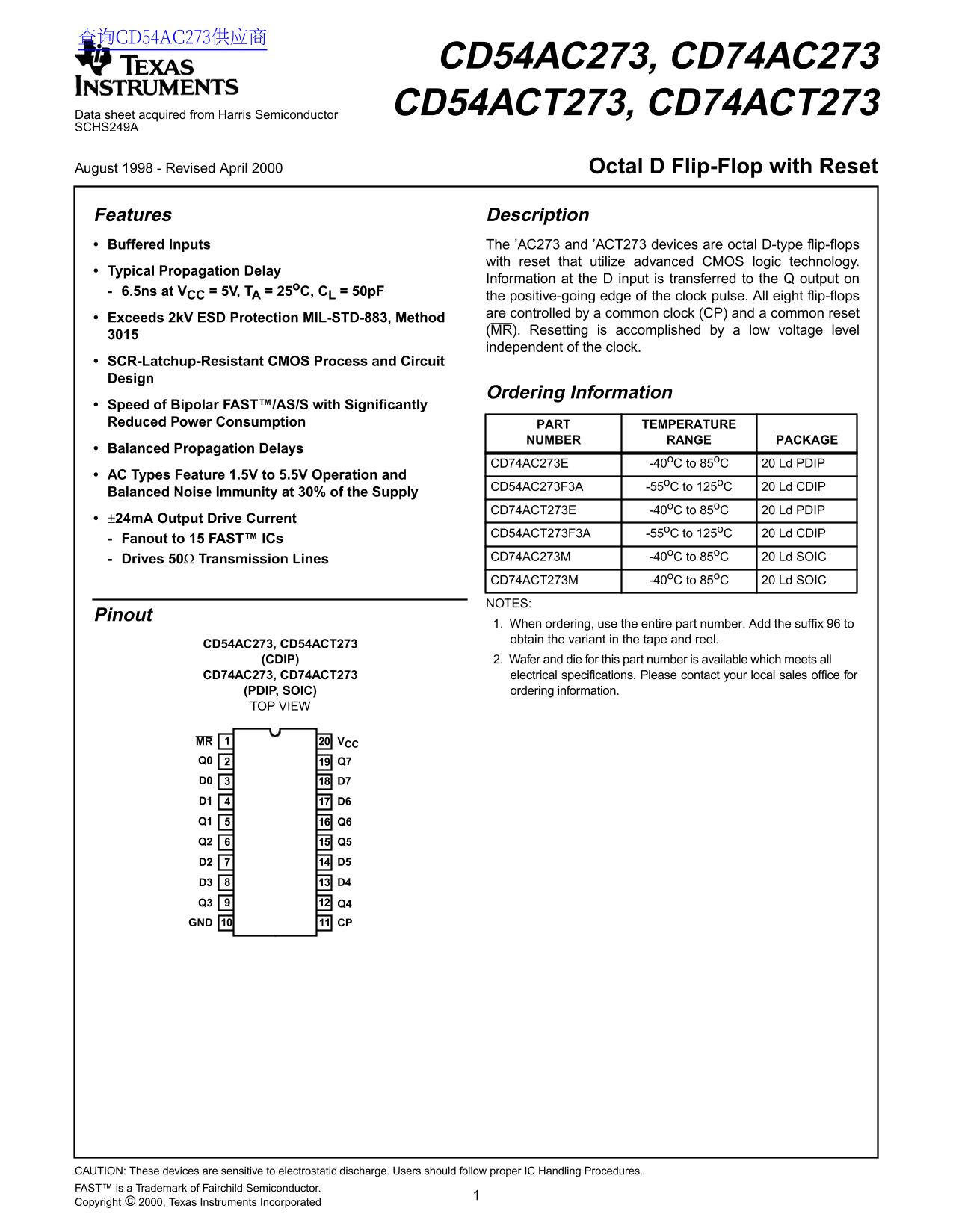
Page 1 Text Content
查询CD54AC273供应商
CD54AC273, CD74AC273 CD54ACT273, CD74ACT273
Data sheet acquired from Harris Semiconductor SCHS249A
August 1998 - Revised April 2000 Octal D Flip-Flop with Reset
Features Description Buffered Inputs The ’AC273 and ’ACT273 devices are octal D-type flip-flops
with reset that utilize advanced CMOS logic technology.
Typical Propagation Delay
Information at the input is transferred to the output on
6.5ns at VCC = 5V, TA = 25o C, CL = 50p F
the positive-going edge of the clock pulse. All eight flip-flops are controlled by common clock (CP) and common reset
Exceeds 2k V ESD Protection MIL-STD-883, Method
(MR). Resetting is accomplished by low voltage level independent of the clock.
SCR-Latchup-Resistant CMOS Process and Circuit Design
Ordering Information
Speed of Bipolar FAST™/AS/S with Significantly Reduced Power Consumption PART TEMPERATURE
NUMBER RANGE PACKAGE
Balanced Propagation Delays
CD74AC273E -40o C to 85o C 20 Ld PDIP
AC Types Feature 1.5V to 5.5V Operation and
CD54AC273F3A -55o C to 125o C 20 Ld CDIP
Balanced Noise Immunity at 30% of the Supply
CD74ACT273E -40o C to 85o C 20 Ld PDIP
±24m A Output Drive Current
CD54ACT273F3A -55o C to 125o C 20 Ld CDIP
Fanout to 15 FAST™ ICs
Drives 50Ω Transmission Lines CD74AC273M -40o C to 85o C 20 Ld SOIC CD74ACT273M -40o C to 85o C 20 Ld SOIC NOTES:
Pinout
1. When ordering, use the entire part number. Add the suffix to obtain the variant in the tape and reel.
CD54AC273, CD54ACT273
(CDIP) 2. Wafer and die for this part number is available which meets all
CD74AC273, CD74ACT273 electrical specifications. Please contact your local sales office for (PDIP, SOIC) ordering information. TOP VIEW
1MR VCC Q0 Q7 D0 D7 D1 D6 Q1 Q6 Q2 Q5
Q3 Q4 GND CP
CAUTION: These devices are sensitive to electrostatic discharge. Users should follow proper IC Handling Procedures. FAST™ is a Trademark of Fairchild Semiconductor. Copyright © 2000, Texas Instruments Incorporated
Page Summary Contents For Texas Instruments CD54AC273, CD74AC273 CD54ACT273, CD74ACT273 Octal D Flip-Flop with Reset Data Sheet User Manual
Manual Details
| Brand | Texas Instruments |
|---|---|
| Pages | 8 |
| File Size | 35.01 KB |
| Published | July 16, 2026 |
Enter the captcha to get the download link:

Frequently Asked Questions
How sensitive are these devices regarding handling?
These devices are highly sensitive to electrostatic discharge (ESD), so users must follow proper IC Handling Procedures.
What determines the operating temperature range for the different types?
The CD74 variants operate from -40°C to 85°C, while the CD54 variants operate in a wider range of -55°C to 125°C.
What is the typical propagation delay time at standard conditions?
The time from D input to Q output is typically 0 - 6.5ns when tested at V=5V, T=25C, and C=50pF.
How should I order the material in a tape and reel format?
When ordering, use the entire part number and add the suffix 96 to obtain the variant in tape and reel.