ST M74HCT273 Octal D Type Flip Flop with Clear Data Sheet Owner's Manual
Summary
The M74HCT273 is a high-speed CMOS Octal D-Type Flip Flop with Clear, providing seven independent output stages for robust digital circuit design. This manual serves as a comprehensive technical resource for hardware engineers and electronic designers, detailing the component's electrical specifications (timing diagrams, propagation delays), operating parameters, mechanical dimensions, and usage guidelines. Ideal for integrating reliable high-speed latching logic into various embedded or digital systems using TTL-compatible interfaces.
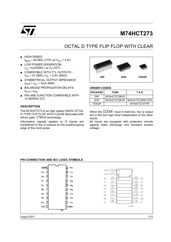
Page 1 Text Content
M74HCT273
OCTAL D TYPE FLIP FLOP WITH CLEAR
HIGH SPEED : f MAX = 80 MHz (TYP.) at VCC = 4.5V LOW POWER DISSIPATION: ICC =4µA(MAX.) at TA=25°C COMPATIBLE WITH TTL OUTPUTS : VIH = 2V (MIN.) VIL = 0.8V (MAX)
SOP TSSOPDIP
SYMMETRICAL OUTPUT IMPEDANCE: |IOH| = IOL = 4m A (MIN) BALANCED PROPAGATION DELAYS: ORDER CODES t PLH ≅ t PHL
PACKAGE TUBE T & R
PIN AND FUNCTION COMPATIBLE WITH
DIP M74HCT273B1R
74 SERIES 273
SOP M74HCT273M1R M74HCT273RM13TR TSSOP M74HCT273TTR
DESCRIPTION The M74HCT273 is an high speed CMOS OCTAL
When the CLEAR input is held low, the Q output
D TYPE FLIP FLOP WITH CLEAR fabricated with
are in the low logic level independent of the other
silicon gate C2MOS technology.
inputs. Information signals applied to D inputs are All inputs are equipped with protection circuits transferred to the Q outputs on the positive-going against static discharge and transient excess edge of the clock pulse. voltage.
PIN CONNECTION AND IEC LOGIC SYMBOLS
1/10August 2001
Page Summary Contents For ST M74HCT273 Octal D Type Flip Flop with Clear Data Sheet Owner's Manual
Manual Details
| Brand | CLEAR |
|---|---|
| Pages | 10 |
| File Size | 267.39 KB |
| Published | May 18, 2026 |
Enter the captcha to get the download link:

Frequently Asked Questions
What function does the CLEAR input perform?
When held low, the Q output is forced into a low logic level, regardless of other inputs.
What is the typical maximum operating frequency?
The device typically operates at up to 80 MHz when Vcc is 4.5V.
What are the recommended supply voltage ranges for operation?
The specified operating voltage range (Vcc) is between 4.5 V and 5.5 V.
Are there limits on data input voltages?
Inputs can accommodate voltages from 0 V to 5.5 V, matching ground up to the supply voltage.