ST M74HC107 Dual J-K Flip-Flop with Clear User Guide
Summary
Discover the M74HC107, a reliable high-speed CMOS dual JK Flip Flop designed for stable digital logic state management. Featuring low power dissipation and wide operational voltage ranges, this component meets stringent performance demands in modern circuits. This manual provides comprehensive technical documentation, covering detailed electrical specifications, timing parameters, application guidelines, and pin compatibility information necessary for reliable design integration. It is essential reading for electronics engineers and circuit designers building robust sequential digital systems.
Page 1 Text Content
M74HC107
DUAL J-K FLIP FLOP WITH CLEAR
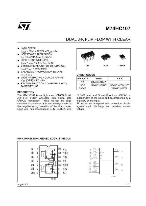
HIGH SPEED : f MAX = 80MHz (TYP.) at VCC = 6V LOW POWER DISSIPATION: ICC =2µA(MAX.) at TA=25°C HIGH NOISE IMMUNITY: VNIH = VNIL = 28 % VCC (MIN.)
SYMMETRICAL OUTPUT IMPEDANCE: SOP TSSOPDIP
|IOH| = IOL = 4m A (MIN) BALANCED PROPAGATION DELAYS: t PLH ≅ t PHL ORDER CODES WIDE OPERATING VOLTAGE RANGE:
PACKAGE TUBE T & R
VCC (OPR) = 2V to 6V
DIP M74HC107B1R
PIN AND FUNCTION COMPATIBLE WITH
SOP M74HC107M1R M74HC107RM13TR
74 SERIES 107
TSSOP M74HC107TTR
DESCRIPTION
The M74HC107 is an high speed CMOS DUAL CLEAR input and Q and Q outputs. CLEAR is J-K FLIP FLOP fabricated with silicon gate independent of the clock and accomplished by a C2MOS technology. These flip-flop are edge logic low on the input. sensitive to the clock input and change state on All inputs are equipped with protection circuits the negative going transition of the clock pulse. against static discharge and transient excess Each one has independent J, K, CLOCK, and voltage.
PIN CONNECTION AND IEC LOGIC SYMBOLS
1/11August 2001
Page Summary Contents For ST M74HC107 Dual J-K Flip-Flop with Clear User Guide
Manual Details
| Brand | CLEAR |
|---|---|
| Pages | 11 |
| File Size | 164.66 KB |
| Published | May 18, 2026 |
Enter the captcha to get the download link:

Frequently Asked Questions
What is the recommended operating voltage range for this flip-flop?
The recommended operating supply voltage (VCC) is between 2 V and 6 V.
How are inputs protected from damage?
All inputs are equipped with protection circuits against static discharge and transient excess current.
What are the minimum timing requirements for input setup and hold times?
The minimum Setup time at 4.5V is 71 ns, while the minimum Hold Time is 0 ns.
Can this component be used in life support systems?
No. STMicroelectronics products are not authorized for use as critical components in life support devices without express written approval.