Texas Instruments SN74F112 Dual Negative-Edge-Triggered J-K Flip-Flop with Clear and Preset
Summary
This integrated circuit provides two independent negative-edge triggered J-K flip-flops, offering essential state storage and data sequencing capabilities for digital logic circuits. The manual serves as a comprehensive technical guide for hardware engineers, detailing critical operational features such as preset and clear inputs, stable clock triggering mechanisms, and full functionality tables. It includes detailed electrical characteristics, absolute maximum ratings across common industrial temperature ranges (0°C to 70°C), dimensional information, and various packaging options, ensuring reliable integration into complex digital system designs.
Page 1 Text Content
SN74F112
DUAL NEGATIVE-EDGE-TRIGGERED J-K FLIP-FLOP
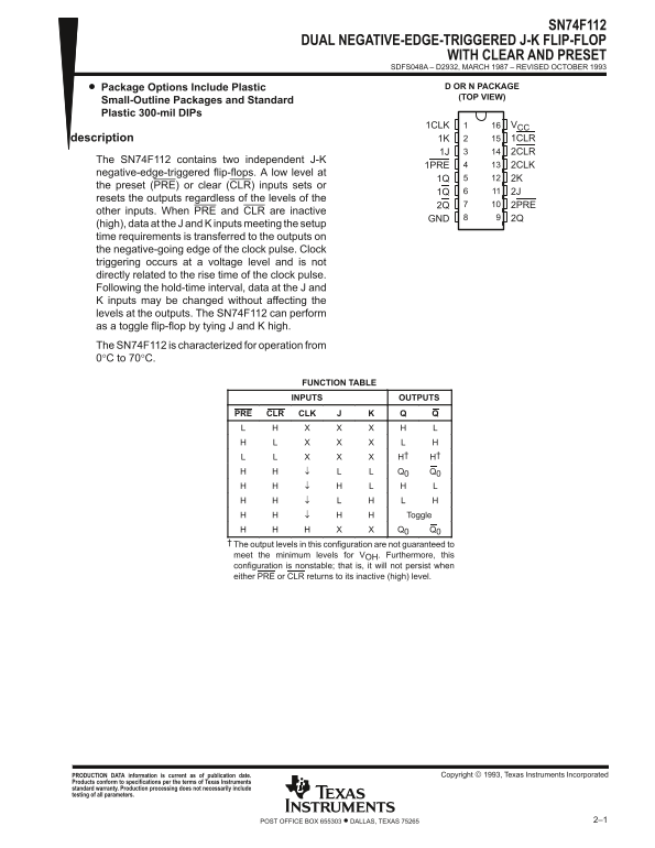
WITH CLEAR AND PRESET SDFS048A – D2932, MARCH 1987 – REVISED OCTOBER 1993 Package Options Include Plastic D OR N PACKAGE (TOP VIEW)
Small-Outline Packages and Standard Plastic 300-mil DIPs
1CLK VCC description 1K 1CLR 1J 2CLR
The SN74F112 contains two independent J-K
1PRE 2CLK
negative-edge-triggered flip-flops. A low level at
the preset (PRE) or clear (CLR) inputs sets or
resets the outputs regardless of the levels of the
2Q 2PRE
other inputs. When PRE and CLR are inactive
GND 2Q
(high), data at the J and K inputs meeting the setup time requirements is transferred to the outputs on the negative-going edge of the clock pulse. Clock triggering occurs at a voltage level and is not directly related to the rise time of the clock pulse. Following the hold-time interval, data at the J and K inputs may be changed without affecting the levels at the outputs. The SN74F112 can perform as a toggle flip-flop by tying J and K high. The SN74F112 is characterized for operation from 0°C to 70°C.
FUNCTION TABLE INPUTS OUTPUTS
PRE CLR CLK
Toggle Q0 Q0
The output levels in this configuration are not guaranteed to meet the minimum levels for VOH. Furthermore, this configuration is nonstable; that is, it will not persist when either PRE or CLR returns to its inactive (high) level.
PRODUCTION DATA information is current as of publication date. Copyright 1993, Texas Instruments Incorporated
Products conform to specifications per the terms of Texas Instruments standard warranty. Production processing does not necessarily include testing of all parameters.
2–1POST OFFICE BOX 655303 • DALLAS, TEXAS 75265
Page Summary Contents For Texas Instruments SN74F112 Dual Negative-Edge-Triggered J-K Flip-Flop with Clear and Preset
Manual Details
| Brand | Texas Instruments |
|---|---|
| Pages | 12 |
| File Size | 477.67 KB |
| Published | June 21, 2026 |
Enter the captcha to get the download link:

Frequently Asked Questions
How do I reset the flip-flop outputs?
A low level at either the preset (PRE) or clear (CLR) input will set the outputs regardless of other inputs.
What is the specific clock triggering mechanism?
The device is negative-edge-triggered, meaning data transfers on the negative-going edge of the clock pulse.
Can this chip be configured to act as a toggle flip-flop?
Yes, it can perform as a toggle flip-flop by tying both the J and K inputs high.
What is the normal operating temperature range?
The SN74F112 is characterized for operation from 0°C to 70°C.