# A B C D E F G H I J K L M N O P Q R S T U V W X Y Z

Siemens PROFET BTS 432 I2 User's Manual

Summary

This Smart Highside Power Switch is a robust, solid-state solution designed to replace traditional electromechanical relays and complex discrete circuits. Featuring advanced SIPMOS technology, it manages 12V and 24V DC grounded loads across various connection types (resistive, inductive, capacitive). The detailed manual highlights its comprehensive protection features, including load dump, short-circuit detection, open load sensing, over/undervoltage monitoring with auto-restart, and diagnostic feedback. It’s ideal for engineers requiring reliable, high-efficiency switching with minimal external components.
📄 Preview PAGE OF 14

Page 1 Text Content

PROFET® BTS 432 I2

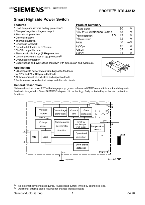
Smart Highside Power Switch Features Product Summary • Load dump and reverse battery protection1)

VLoad dump

• Clamp of negative voltage at output

Vbb-VOUT Avalanche Clamp

• Short-circuit protection

Vbb (operation) 4.5 ... 42

• Current limitation

Vbb (reverse) -32

• Thermal shutdown

RON mΩ

• Diagnostic feedback

IL(SCp)

• Open load detection in OFF-state

• CMOS compatible input IL(SCr) • Electrostatic discharge (ESD) protection IL(ISO)

• Loss of ground and loss of Vbb protection2) • Overvoltage protection • Undervoltage and overvoltage shutdown with auto-restart and hysteresis

Application • µC compatible power switch with diagnostic feedback for 12 V and 24 V DC grounded loads • All types of resistive, inductive and capacitve loads • Replaces electromechanical relays and discrete circuits

General Description N channel vertical power FET with charge pump, ground referenced CMOS compatible input and diagnostic feedback, integrated in Smart SIPMOS chip on chip technology. Fully protected by embedded protection functions.

+ Vbb

Voltage

Overvoltage Current Gate

source protection limit protection

Logic

Voltage Charge pump Limit for unclamped

sensor Level shifter Temperature

ind. loads

sensor Rectifier

Open load

ESD Logic detection

Short circuit detection

GND PROFET

Signal GND Load GND

1) No external components required, reverse load current limited by connected load. 2) Additional external diode required for charged inductive loads

Semiconductor Group 04.96

Page Summary Contents For Siemens PROFET BTS 432 I2 User's Manual

Page 1 PROFET® BTS 432 I2 Smart Highside Power Switch Features Product Summary • Load dump and reverse battery protection1) VLoad dump • Clamp of negative voltage at output Vbb-VOUT Avalanche Clamp • Short-c...
Page 2 BTS 432 I2 Pin Symbol Function GND Logic ground IN Input, activates the power switch in case of logical high signal Vbb Positive power supply voltage, the tab is shorted to this pin ST Diagnostic feed...
Page 3 BTS 432 I2 Electrical Characteristics Parameter and Conditions Symbol Values Unit at Tj = 25 °C, Vbb = 12 V unless otherwise specified min typ max Load Switching Capabilities and Characteristics On-st...
Page 4 BTS 432 I2 Parameter and Conditions Symbol Values Unit at Tj = 25 °C, Vbb = 12 V unless otherwise specified min typ max Protection Functions Initial peak short circuit current limit (pin 3 to 5)8), IL...
Page 5 BTS 432 I2 Parameter and Conditions Symbol Values Unit at Tj = 25 °C, Vbb = 12 V unless otherwise specified min typ max Input and Status Feedback11) Input turn-on threshold voltage VIN(T+) 1.5 2.4 Tj ...
Page 6 BTS 432 I2 Truth Table Input- Output Status level level Normal operation Open load Short circuit to GND Short circuit to Vbb H (L15)) H (L15)) Overtem- perature Under- L16) L16) voltage L16) L16) Over...
Page 7 BTS 432 I2 Inductive and overvoltage output clamp GND disconnect + Vbb ON bb PROFET OUT bb IN VGND VON clamped to 58 V typ. Overvolt. and reverse batt. protection Any kind of load. In case of Input=hi...
Page 8 BTS 432 I2 Inductive Load switch-off energy dissipation bb ELoad PROFET Energy dissipated in PROFET EAS = Ebb + EL - ER. ELoad < EL, EL = 1/2 * L * I2L Semiconductor Group
Page 9 BTS 432 I2 Options Overview all versions: High-side switch, Input protection, ESD protection, load dump and reverse battery protection , protection against loss of ground Type BTS 432D2 432E2 432F2 43...
Page 10 BTS 432 I2 Timing diagrams Figure 1a: Vbb turn on: Figure 2b: Switching an inductive load d(bb IN) ST CMOS in case of too early VIN=high the device may not turn on (curve A) td(bb IN) approx. 150 µs F...
Page 11 BTS 432 I2 Figure 3b: Turn on into overload, Figure 4a: Overtemperature, Reset if (IN=low) and (Tj<Tjt) L(SCp)I L(SCr)I Heating up may require several milliseconds , Vbb - VOUT < 8.3 V typ. *) S...
Page 12 BTS 432 I2 Figure 5b: Open load: detection in OFF-state, turn Figure 6a: Undervoltage: on/off to open load d(ST OL3) bb(u cp) bb(under) bb(u rst) ST CMOS open normal in case of external capacity td(ST...
Page 13 BTS 432 I2 Figure 7a: Overvoltage: Vbb(over) Vbb(o rst) ON(CL)V Semiconductor Group
Page 14 BTS 432 I2 Package and Ordering Code All dimensions in mm Standard TO-220AB/5 Ordering code SMD TO-220AB/5, Opt. E3122 Ordering code BTS 432 I2 Q67060-S6204-A2 BTS 432 I2 E3122A T&R: Q67060-S6204-...