ROHM BD3538F Data Handbook/Manual
Summary
The BD3538F/HFN is a high-performance termination regulator for DDR-SDRAMs. This linear power supply offers 1A sink/source current and excellent transient response, operating with a 2.7V to 5.5V input. It is designed for power supply applications in PCs and general electronic equipment.
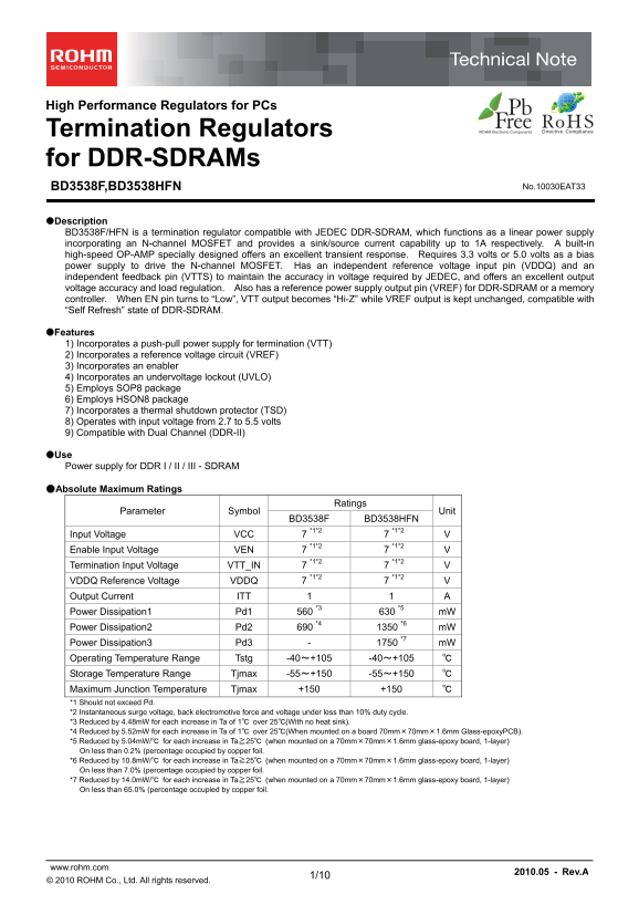
Page 1 Text Content
High Performance Regulators for PCs
Termination Regulators for DDR-SDRAMs
BD3538F,BD3538HFN No.10030EAT33
Description BD3538F/HFN is a termination regulator compatible with JEDEC DDR-SDRAM, which functions as a linear power supply incorporating an N-channel MOSFET and provides a sink/source current capability up to 1A respectively. A built-in high-speed OP-AMP specially designed offers an excellent transient response. Requires 3.3 volts or 5.0 volts as a bias power supply to drive the N-channel MOSFET. Has an independent reference voltage input pin (VDDQ) and an independent feedback pin (VTTS) to maintain the accuracy in voltage required by JEDEC, and offers an excellent output voltage accuracy and load regulation. Also has a reference power supply output pin (VREF) for DDR-SDRAM or a memory controller. When EN pin turns to “Low”, VTT output becomes “Hi-Z” while VREF output is kept unchanged, compatible with “Self Refresh” state of DDR-SDRAM.
Features 1) Incorporates a push-pull power supply for termination (VTT) 2) Incorporates a reference voltage circuit (VREF) 3) Incorporates an enabler 4) Incorporates an undervoltage lockout (UVLO) 5) Employs SOP8 package 6) Employs HSON8 package 7) Incorporates a thermal shutdown protector (TSD) 8) Operates with input voltage from 2.7 to 5.5 volts 9) Compatible with Dual Channel (DDR-II)
Use Power supply for DDR I / II / III - SDRAM
●Absolute Maximum Ratings
Ratings
Parameter Symbol Unit
BD3538F BD3538HFN
Input Voltage VCC 7 *1*2 7 *1*2 V Enable Input Voltage VEN 7 *1*2 7 *1*2 V Termination Input Voltage VTT_IN 7 *1*2 7 *1*2 V VDDQ Reference Voltage VDDQ 7 *1*2 7 *1*2 V Output Current ITT 1 1 A Power Dissipation1 Pd1 560 *3 630 *5 m W Power Dissipation2 Pd2 690 *4 1350 *6 m W Power Dissipation3 Pd3 - 1750 *7 m W Operating Temperature Range Tstg -40~+105 -40~+105 ℃ Storage Temperature Range Tjmax -55~+150 -55~+150 ℃ Maximum Junction Temperature Tjmax +150 +150 ℃ *1 Should not exceed Pd. *2 Instantaneous surge voltage, back electromotive force and voltage under less than 10% duty cycle. *3 Reduced by 4.48m W for each increase in Ta of 1℃ over 25℃(With no heat sink). *4 Reduced by 5.52m W for each increase in Ta of 1℃ over 25℃(When mounted on a board 70mm×70mm×1.6mm Glass-epoxy PCB). *5 Reduced by 5.04m W/℃ for each increase in Ta≧25℃ (when mounted on a 70mm×70mm×1.6mm glass-epoxy board, 1-layer) On less than 0.2% (percentage occupied by copper foil. *6 Reduced by 10.8m W/℃ for each increase in Ta≧25℃ (when mounted on a 70mm×70mm×1.6mm glass-epoxy board, 1-layer) On less than 7.0% (percentage occupied by copper foil. *7 Reduced by 14.0m W/℃ for each increase in Ta≧25℃ (when mounted on a 70mm×70mm×1.6mm glass-epoxy board, 1-layer) On less than 65.0% (percentage occupied by copper foil.
www.rohm.com 2010.05 - Rev.A
© 2010 ROHM Co., Ltd. All rights reserved.
Page Summary Contents For ROHM BD3538F Data Handbook/Manual
Manual Details
| Brand | ROHM |
|---|---|
| Pages | 11 |
| File Size | 383.30 KB |
| Published | June 15, 2026 |
Enter the captcha to get the download link:

Frequently Asked Questions
What happens when the EN pin is set to Low?
VTT output becomes Hi-Z while VREF output remains unchanged, compatible with the Self Refresh state of DDR-SDRAM.
What is the input voltage range for VCC?
The input voltage (VCC) can range from 2.7V to 5.5V.
What is the maximum sink/source current capability?
The BD3538F/HFN can sink or source up to 1A respectively.
Does this product have radiation-resistant design?
No, radiation-resistant design is not adopted for this product.