# A B C D E F G H I J K L M N O P Q R S T U V W X Y Z

ROHM BD2066FJ Data Manual

Summary

Advanced dual N-MOS high-side power switches designed for reliable power management in sensitive digital circuits. These ICs include crucial built-in protections such as over-current detection, thermal shutdown, and under-voltage lockout. Ideal for engineers developing PC peripherals, USB hubs, consumer appliances, and car accessories that require robust and controlled power switching capability. The associated manual provides detailed electrical characteristics, operating conditions, and technical guidelines necessary for optimal product integration into complex electronic systems.
📄 Preview PAGE OF 17

Page 1 Text Content

Power Management Switch ICs for PCs and Digital Consumer Products

2ch High Side Switch ICs for USB Devices and Memory Cards

BD2062FJ,BD2066FJ No.11029EBT15

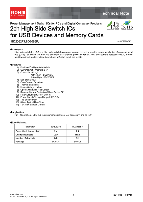
●Description High side switch for USB is a high side switch having over-current protection used in power supply line of universal serial bus (USB). Its switch unit has two channels of N-channel power MOSFET. And, over-current detection circuit, thermal shutdown circuit, under-voltage lockout and soft-start circuit are built in.

●Features 1) Dual N-MOS High Side Switch 2) Current Limit Threshold 2.4A 3) Control Input Logic Active-Low : BD2062FJ Active-High : BD2066FJ 4) Soft-Start Circuit 5) Over-Current Detection 6) Thermal Shutdown 7) Under-Voltage Lockout 8) Open-Drain Error Flag Output 9) Reverse Current Protection When Switch Off 10) Flag Output Delay Filter Built In 11) Power Supply Voltage Range 2.7V~5.5V 12) TTL Enable Input 13) 0.8ms Typical Rise Time 14) 1μA Max Standby Current

●Applications PC, PC peripheral USB hub in consumer appliances, Car accessory, and so forth

●Line Up Matrix

Parameter BD2062FJ BD2066FJ

Current limit threshold (A) 2.4 2.4 Control input logic Low High Number of channels 2ch 2ch Package SOP-J8 SOP-J8

www.rohm.com 2011.05 - Rev.B

© 2011 ROHM Co., Ltd. All rights reserved.

Page Summary Contents For ROHM BD2066FJ Data Manual

Page 1 Power Management Switch ICs for PCs and Digital Consumer Products 2ch High Side Switch ICs for USB Devices and Memory Cards BD2062FJ,BD2066FJ No.11029EBT15 ●Description High side switch for USB is a h...
Page 2 BD2062FJ,BD2066FJ Technical Note ●Absolute Maximum Ratings (Ta=25℃) Parameter Symbol Ratings Unit Supply voltage VIN -0.3 ~ 6.0 V Enable input voltage VEN -0.3 ~ 6.0 V /OC voltage V/OC -0.3 ~ 6.0 V /O...
Page 3 BD2062FJ,BD2066FJ Technical Note ●Electrical Characteristics ○BD2062FJ (Unless otherwise specified VIN = 5.0V, Ta = 25℃) Limits Parameter Symbol Unit Conditions Min. Typ. Max. Operating current IDD - ...
Page 4 BD2062FJ,BD2066FJ Technical Note ○BD2066FJ (Unless otherwise specified VIN = 5.0V, Ta = 25 ℃) Limits Parameter Symbol Unit Condition Min. Typ. Max. Operating current IDD - 130 180 μA VEN = 5V , OUT=OP...
Page 5 BD2062FJ,BD2066FJ Technical Note ●Measurement Circuit VIN VIN 1µF 1µF GND /OC1 GND /OC1 IN OUT1 IN OUT1 RL CL VEN EN1 OUT2 VEN EN1 OUT2 RL CL VEN EN2 /OC2 VEN EN2 /OC2 Operating current EN, /EN input ...
Page 6 BD2062FJ,BD2066FJ Technical Note /O /O IN u A IS : I ●Electrical Characteristic Curves (Reference Data) TA=25℃ TA=25℃ VIN=5V SUPPLY VOLTAGE: VIN (V) AMBIENT TEMPERATURE: TA (℃) SUPPLY VOLTAGE: VIN (V)...
Page 7 BD2062FJ,BD2066FJ Technical Note IM us IM (u s) IS IM s) IS IM s) TA=25℃ TA=25℃ VIN=5V SUPPLY VOLTAGE: VIN (V) AMBIENT TEMPERATURE: TA (℃) SUPPLY VOLTAGE: VIN (V) Fig.16 Short circuit current Fig.17 S...
Page 8 BD2062FJ,BD2066FJ Technical Note VUVLOH VUVLOL 0.05 AMBIENT TEMPERATURE: TA(℃) AMBIENT TEMPERATURE: TA(℃) Fig.28 UVLO threshold voltage Fig.29 UVLO hysteresis voltage IS (V ●Waveform Data(BD2062FJ) /E...
Page 9 BD2062FJ,BD2066FJ Technical Note ●Block Diagram /EN1 TSD1 EN1 /OC1 Gate Delay Logic1 Charge Pump1 IN OUT1 GND /OC1 /EN2 IN OUT1 EN2 Top View Charge Pump2 3/EN1 OUT2 (EN1) Gate /OC2 Logic2 Delay /OC2 G...
Page 10 BD2062FJ,BD2066FJ Technical Note ●I/O Circuit Symbol Pin No Equivalent circuit /EN1(EN1) /EN2(EN2) EN1(/EN1) EN2(/EN2) 3, 4 /OC1 /OC2 /OC1 /OC2 5, 8 OUT1 OUT1 OUT2 OUT2 6, 7 www.rohm.com 2011.05 - Rev...
Page 11 BD2062FJ,BD2066FJ Technical Note ●Functional Description 1. Switch operation IN terminal and OUT terminal are connected to the drain and the source of switch MOSFET respectively. And the IN terminal i...
Page 12 BD2062FJ,BD2066FJ Technical Note 5. Error flag (/OC) output Error flag output is N-MOS open drain output. At detection of over-current, thermal shutdown, low level is output. Over-current detection ha...
Page 13 BD2062FJ,BD2066FJ Technical Note ●Typical Application Circuit 5V(Typ.) Ferrite Beads OUTIN ON/OFF GND /OC1 D+ CL OC IN OUT1 OC OUT2 Regulator (EN1) GND Data ON/OFF /OC2 (EN2) CL Data BD2062FJ/66FJ USB...
Page 14 BD2062FJ,BD2066FJ Technical Note ●Power Dissipation Character (SOP-J8) IS IP IO : P [m AMBIENT TEMPERATURE: Ta [℃] Fig.43 Power dissipation curve (Pd-Ta Curve) ●Notes for use (1) Absolute Maximum Rati...
Page 15 BD2062FJ,BD2066FJ Technical Note (7) Operation in strong electromagnetic field Be noted that using ICs in the strong electromagnetic field can malfunction them. (8) Inspection with set PCB On the insp...
Page 16 BD2062FJ,BD2066FJ Technical Note ●Ordering part number Part No. Part No. Package Packaging and forming specification FJ: SOP-J8 E2: Embossed tape and reel SOP-J8 <Tape and Reel information> (MAX...
Page 17 Notice No copying or reproduction of this document, in part or in whole, is permitted without the consent of ROHM Co.,Ltd. The content specified herein is subject to change for improvement without not...

Manual Details

Brand ROHM
Pages 17
File Size 322.30 KB
Published June 20, 2026
5 views

Enter the captcha to get the download link:

captcha

Frequently Asked Questions

What types of protection features are built into this high side switch?

It includes over-current detection, thermal shutdown circuit, under-voltage lockout, reverse current protection when switched off, and a soft-start circuit.

What is the required power supply voltage range (VIN) for operation?

The operating voltage must be between 2.7V minimum and 5.5V maximum.

In what applications can this device be used?

It is suitable for PCs, PC peripheral USB hubs in consumer appliances, car accessories, and similar electronic equipment.

Are there any situations where this product should not be used?

This product is not designed or rated for use in systems requiring extremely high reliability, such as medical instruments or aerospace machinery.