ROHM BD5426EFS Data Manual
Summary
Dramatically size-reduce your audio equipment with this high-efficiency 10W+10W Class-D power amplifier IC. Designed for low heat dissipation and space-saving applications like smart TVs and portable audio devices, it ensures robust, high-quality sound without bulky cooling systems. The accompanying technical documentation provides complete electrical characteristics, operating parameters, efficiency grades, and safety guidelines necessary for engineers designing cutting-edge consumer electronics.
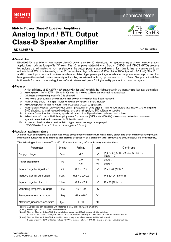
Page 1 Text Content
Middle Power Class-D Speaker Amplifiers
Analog Input / BTL Output Class-D Speaker Amplifier
No.10075EBT05
BD5426EFS
●Description BD5426EFS is a 10W + 10W stereo class-D power amplifier IC, developed for space-saving and low heat-generation applications such as low-profile TV sets. The IC employs state-of-the-art Bipolar, CMOS, and DMOS (BCD) process technology that eliminates turn-on resistance in the output power stage and internal loss due to line resistances up to an ultimate level. With this technology, the IC has achieved high efficiency of 87% (9W + 9W output with 8Ω load). The IC, in addition, employs a compact back-surface heat radiation type power package to achieve low power consumption and low heat generation and eliminates necessity of installing an external radiator, up to a total output of 20W. This product satisfies both needs for drastic downsizing, low-profile structures and powerful, high-quality playback of the sound system.
●Features 1) A high efficiency of 87% (9W + 9W output with 8Ω load), which is the highest grade in the industry and low heat-generation. 2) An output of 10W + 10W (13V, with 8Ω load) is allowed without an external heat radiator. 3) Driving a lowest rating load of 6Ω is allowed. 4) Pop noise upon turning power on/off and power interruption has been reduced. 5) High-quality audio muting is implemented by soft-switching technology. 6) An output power limiter function limits excessive output to speakers. 7) High-reliability design provided with built-in protection circuits against high temperatures, against VCC shorting and
GND shorting, against reduced-voltage, and against applying DC voltage to speaker. 8) A master/slave function allowing synchronization of multiple devices reduces beat noises. 9) Adjustment of internal PWM sampling clock frequencies (250k Hz to 400k Hz) allows easy protective measures against unwanted radio emission to AM radio band. 10) A compact back-surface heat radiation type power package is employed. HTSSOP-A44(5mm × 7.5mm × 1.0mm, pitch 0.8mm )
●Absolute maximum ratings A circuit must be designed and evaluated not to exceed absolute maximum rating in any cases and even momentarily, to prevent reduction in functional performances and thermal destruction of a semiconductor product and secure useful life and reliability. The following values assume Ta =25℃. For latest values, refer to delivery specifications.
Parameter Symbol Ratings Unit Conditions
Supply voltage VCC +20 V Pin 7, 8, 15, 16, 29, 30, 37, 38, 40
(Note 1, 2)
2.0 (Note 3)
Power dissipation Pd
4.5 (Note 4)
Input voltage for signal pin VIN -0.2 ~ +7.2 V Pin 1, 44 (Note 1)
Input voltage for control pin VCONT -0.2 ~ Vcc+0.2 V Pin 20, 24 (Note 1)
Input voltage for clock pin VOSC -0.2 ~ +7.2 V Pin 23 (Note 1)
Operating temperature range Topr -40 ~ +85 ℃
Storage temperature range Tstg -55 ~ +150 ℃
Maximum junction temperature Tjmax +150 ℃ (Note 1) A voltage that can be applied with reference to GND (pins 11, 12, 33, 34, and 43) (Note 2) Pd and Tjmax=150℃ must not be exceeded. (Note 3) 70mm × 70mm × 1.6mm FR4 One-sided glass epoxy board (Back copper foil 0%) installed. If used under Ta=25℃ or higher, reduce 16m W for increase of every 1℃. The board is provided with thermal via. (Note 4) 70mm × 70mm × 1.6mm FR4 Both-sided glass epoxy board (Back copper foil 100%) installed. If used under Ta=25℃ or higher, reduce 36m W for increase of every 1℃. The board is provided with thermal via.
1/16 www.rohm.com 2010.05 - Rev.B
© 2010 ROHM Co., Ltd. All rights reserved.
Page Summary Contents For ROHM BD5426EFS Data Manual
Manual Details
| Brand | ROHM |
|---|---|
| Pages | 17 |
| File Size | 523.12 KB |
| Published | June 04, 2026 |
Enter the captcha to get the download link:

Frequently Asked Questions
What is the maximum continuous output power without external cooling?
It can handle a total output of 20W thanks to its compact back-surface heat radiation package, eliminating the need for an external radiator.
How efficient is this Class-D amplifier during operation?
The IC features a high efficiency rating of 87% when providing a 9W + 9W output with an 8Ω load.
What safety protections are built into the circuit design?
It has multiple built-in protection circuits covering high temperatures, VCC shorting, GND shorting, reduced voltage, and DC voltage on speakers.
What is the allowable range for load resistance (RL)?
The operating conditions specify that the load resistance must be between 6 Ω and 16 Ω.