ROHM BD8143MUV Data Manual
Summary
This high-precision Gamma Correction IC provides a comprehensive, single-chip solution with built-in DACs and multiple amplification channels for TFT LCD panels. Ideal for engineers developing large-screen and HD TV displays, this module offers setting control via serial communication, reducing board complexity and ensuring superior image quality. The manual details complete technical specifications, operational parameters, and application guidelines needed for seamless integration into next-generation display systems.
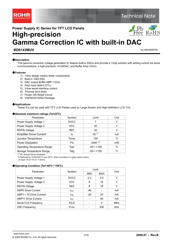
Page 1 Text Content
Power Supply IC Series for TFT LCD Panels
High-precision Gamma Correction IC with built-in DAC
BD8143MUV No.09035EBT08
●Description This gamma correction voltage generation IC feature built-in DACs and provide a 1chip solution with setting control via serial communications, a high-precision 10-bit DAC, and Buffer Amp (12ch).
●Features 1) 1chip design means fewer components 2) Built-in 10bit DAC 3) DAC output Buffer AMP (12ch) 4) Amp input select (CTL) 5) 3-line serial interface control 6) Thermal shut down 7) Power ON Reset Circuit 8) VQFN032V5050 Package
●Applications These ICs can be used with TFT LCD Panels used by Large-Screen and High-Definition LCD TVs.
●Absolute maximum ratings (Ta=25℃)
Parameter Symbol Limit Unit
Power Supply Voltage 1 DVCC 7 V Power Supply Voltage 2 VCC 20 V REFIN Voltage REF 20 V Amplifier Drive Current Io 30 *1 m A Junction Temperature Tjmax 150 ℃ Power Dissipation Pd 2440 *2 m W Operating Temperature Range Topr -40~+105 ℃ Storage Temperature Range Tstg -55~+150 ℃ *1 Pd, should not be exceeded. *2 Reduced by 19.52m W/°C over 25°C, when mounted on a glass epoxy board. (4-layer 74.2×74.2×1.6mm).
●Operating Condition (Ta=-40℃~105℃)
Limit
Parameter Symbol Unit
MIN MAX
Power Supply Voltage 1 DVCC 2.3 5.5 V Power Supply Voltage 2 VCC 8 18 V REFIN Voltage REF 8 18 V AMP0 Drive Current IOA -40 - m A AMP1~10 Drive Current IOB -20 20 m A AMP11 Drive Current IOC - 40 m A Serial CLK Frequency f CLK - 5 MHz OSC Frequency FOSC - 200 k Hz
www.rohm.com 2009.07 - Rev.B
© 2009 ROHM Co., Ltd. All rights reserved.
Page Summary Contents For ROHM BD8143MUV Data Manual
Manual Details
| Brand | ROHM |
|---|---|
| Pages | 11 |
| File Size | 326.12 KB |
| Published | June 02, 2026 |
Enter the captcha to get the download link:

Frequently Asked Questions
What types of devices are these ICs designed to power?
They can be used with TFT LCD Panels intended for Large-Screen and High-Definition LCD TVs.
How is the gamma correction voltage adjusted or controlled?
It provides setting control via a three-line serial communication interface, featuring built-in DACs and Buffer Amps.
What are the required operating voltage ranges (MIN/MAX)?
DVCC must be between 2.3V and 5.5V; VCC and REF tension range from 8V to 18V.
Are these products suitable for safety-critical applications?
No, the products are not designed or manufactured for use in equipment that requires an extremely high level of reliability.