# A B C D E F G H I J K L M N O P Q R S T U V W X Y Z

ROHM BD8919FV Data Manual

Summary

This advanced IC Card Interface solution is essential for connecting 5V smart cards to host controllers. It functions as a highly reliable bidirectional signal buffer, providing necessary power supply (VCC) while offering robust protection against ESD ($\ge \pm 6000$V), short circuits, and over-current events. The integrated manual details key features, including automated activation/deactivation sequences and programmable clock division ratios. Ideal for designers working on CLASS A or B-CAS card applications, this chip ensures stable and secure communication between the card and system electronics.
📄 Preview PAGE OF 16

Page 1 Text Content

IC Card Interface ICs

IC Card Interface ICs with Built-in Low Noise LDO Regulator

BD8918F,BD8918FV,BD8919F,BD8919FV No.09056EDT01

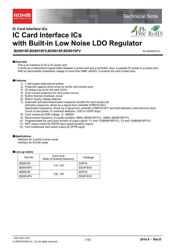
●Overview This is an interface IC for a 5V smart card. It works as a bidirectional signal buffer between a smart card and a controller. Also, it supplies 5V power to a smart card. With an electrostatic breakdown voltage of more than HBM; ±6000V, it protects the card contact pins.

●Features 1) 1 half duplex bidirectional buffers 2) Protection against short-circuit for all the card contact pins 3) 5V power source for the card (VCC) 4) Over-current protection for card power source 5) Built-in thermal shutdown circuit 6) Built-in supply voltage detector 7) Automatic activation/deactivation sequence function for card contact pin Activation sequence: driven by a signal from controller (CMDVCCB) Deactivation sequence: driven by a signal from controller (CMDVCCB) and fault detection (card removal, short

circuit of card power, IC overheat detection, VDD or VDDP drop) 8) Card contact pin ESD voltage ≧ ±6000V 9) Recommend frequency of crystal oscillator: 8MHz (BD8918F/FV), 16MHz (BD8919F/FV) 10) Programmable for card clock division of output signal: 1/1 and 1/2(BD8918F/FV), 1/2 and 1/4(BD8919F/FV). 11) RST output control by RSTIN input signal (positive output) 12) One multiplexed card status output by OFFB signal

●Applications Interface for CLASS A smart cards Interface for B-CAS cards

●Line up matrix

Card clock

Part No

Ratio of dividing frequency Package

BD8918F SOP16

BD8918FV SSOP-B16 BD8919F SOP16

BD8919FV SSOP-B16

www.rohm.com 2010.4 - Rev.D

© 2009 ROHM Co., Ltd. All rights reserved.

Page Summary Contents For ROHM BD8919FV Data Manual

Page 1 IC Card Interface ICs IC Card Interface ICs with Built-in Low Noise LDO Regulator BD8918F,BD8918FV,BD8919F,BD8919FV No.09056EDT01 ●Overview This is an interface IC for a 5V smart card. It works as a b...
Page 2 BD8918F,BD8918FV,BD8919F,BD8919FV Technical Note ●Absolute maximum ratings (Ta=25°C) Parameter Symbol Ratings Unit Notes VDD Input Voltage VDD -0.3 ~ 6.5 V VDDP Input Voltage VDDP -0.3 ~ 6.5 V I/O Pin...
Page 3 BD8918F,BD8918FV,BD8919F,BD8919FV Technical Note ●Block Diagram VDD 10µF0.1u F VIREF TSD ALARM LVS POWER_ON VDD VCC 5V ALARM VCCEN OFFB LDO VCC ALARM RSTIN IO CGND 50k SEQUENCER RSTEN RST BUFLV LV RST...
Page 4 BD8918F,BD8918FV,BD8919F,BD8919FV Technical Note ●Pin Description Pin No. Pin Name I/O Signal Level Pin Function 1 XTAL1 I VDD Crystal connection or input for external clock 2 XTAL2 O VDD Crystal conn...
Page 5 BD8918F,BD8918FV,BD8919F,BD8919FV Technical Note ●Pin Function Diagram Pin Pin Pin Pin Pin function Diagram Pin function Diagram No. Name No. Name VDD VDD VDDP VREG VREG XTAL1 XTAL2 VREG VDDP VDD RST ...
Page 6 BD8918F,BD8918FV,BD8919F,BD8919FV Technical Note Pin No. Pin Name Pin function Diagram Pin No. Pin Name Pin function Diagram 0K VDD VDDP OFFB VDD VDD VDD VDD PRES CMDVCCB www.rohm.com 2010.4 - Rev.D ©...
Page 7 BD8918F,BD8918FV,BD8919F,BD8919FV Technical Note ●Package Package Name: SOP16 Note : X is 8 or 9. (MAX 10.35 include BURR) 0. BD891XF Lot No. 1PIN MARK (UNIT : mm) Fig. 3.1 SOP16 Package Dimension Pac...
Page 8 BD8918F,BD8918FV,BD8919F,BD8919FV Technical Note ●Function 1) Power supply Power supply pins are VDD and VDDP. Set VDD at the same voltage as the signal from the system controller side. VDDP and CGND ...
Page 9 BD8918F,BD8918FV,BD8919F,BD8919FV Technical Note 3-3) Activation sequence When OFFB is in the “High” state and the CMDVCCB signal from the controller turns from H to L, the activation sequence starts ...
Page 10 BD8918F,BD8918FV,BD8919F,BD8919FV Technical Note 3-4) Deactivation sequence When the CMDVCCB input turns from L to H or the alarm signal (described later) is detected, the following deactivation seque...
Page 11 BD8918F,BD8918FV,BD8919F,BD8919FV Technical Note 6) Card clock supply Card clock is supplied from the CLK pin dividing the input frequency of XTAL1 pin with the CLKSEL pin setting. The clock division ...
Page 12 BD8918F,BD8918FV,BD8919F,BD8919FV Technical Note ●An example of software control Start No (No card) OFFB=H ? Yes (Card detect) Error message 1 ・Card insert CMDVCCB: H→L Activation start Regulator on (...
Page 13 BD8918F,BD8918FV,BD8919F,BD8919FV Technical Note ●Application examples BD8918F/FV application examples CONTROLLER XTAL1 GND XTAL2 CMDVCCB 220Ω VDD OFFB CLKSEL BD8918F/ PRES BD8918FV RSTIN VDDP IO_U VC...
Page 14 BD8918F,BD8918FV,BD8919F,BD8919FV Technical Note BD8919F/FV application examples CONTROLLER XTAL1 GND (22p F) 16MHz XTAL2 CMDVCCB 220Ω VDD OFFB CLKSEL PRES BD8919F/ RSTIN BD8919FV VDDP IO_U VCC CGND C...
Page 15 BD8918F,BD8918FV,BD8919F,BD8919FV Technical Note  Ordering part number Part No. Part No. Package Packaging and forming specification E2: Embossed tape and reel F: SOP16 FV: SSOP-B16 SOP16 <Tape an...
Page 16 Notice No copying or reproduction of this document, in part or in whole, is permitted without the consent of ROHM Co.,Ltd. The content specified herein is subject to change for improvement without not...

Manual Details

Brand ROHM
Pages 16
File Size 373.54 KB
Published May 31, 2026
66 views

Enter the captcha to get the download link:

captcha

Frequently Asked Questions

What is the primary function of this interface IC?

It acts as a bidirectional signal buffer and supplies 5V power to a smart card for CLASS A or B-CAS applications.

How does the IC protect the smart card?

It protects against short circuits, has built-in thermal shutdown, and features ESD protection up to ±6000V on the contact pins.

What voltage ranges are used for VDD and VDDP input?

VDD Input Voltage operates between -0.3 V and 6.5 V, while VDDP Input Voltage also uses a range of -0.3 V to 6.5 V.

Can the clock output frequency be customized?

Yes, the BD8918F/FV can divide the signal by 1/1 or 1/2, and the BD8919F/FV can select 1/2 or 1/4 division ratios.