ROHM 2SD1383K Specifications User Guide
Summary
This high-gain bipolar junction transistor provides robust amplification using a Darlington connection structure. This comprehensive manual is an essential resource for electrical engineers, detailing all required specifications including absolute maximum ratings, dynamic performance graphs, current transfer ratios ($h_{FE}$), and breakdown voltage curves across various temperatures. It is the ideal component for developers creating general electronic equipment, from audio-visual devices to sophisticated communication systems requiring stable output power.
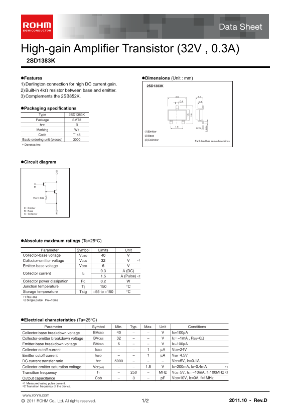
Page 1 Text Content
High-gain Amplifier Transistor (32V , 0.3A) 2SD1383K Features Dimensions (Unit : mm) 1) Darlington connection for high DC current gain.
2SD1383K
2) Built-in 4k resistor between base and emitter. 3) Complements the 2SB852K.
Packaging specifications
Type 2SD1383K Package SMT3
Marking W∗
(1)Emitter
Code T146 (2)Base
Basic ordering unit (pieces) (3)Collector
Each lead has same dimensions
∗ Denotes h FE
Circuit diagram
RBE 4kΩ
E : Emitter B : Base C : Collector
Absolute maximum ratings (Ta=25C)
Parameter Symbol Limits Unit
Collector-base voltage VCBO
Collector-emitter voltage VCES ∗1
Emitter-base voltage VEBO
0.3 A (DC)
Collector current IC
1.5 A (Pulse) ∗2
Collector power dissipation PC 0.2
Junction temperature Tj °C Storage temperature Tstg −55 to +150 °C ∗1 RBE=0Ω ∗2 Single pulse Pw=10ms
Electrical characteristics (Ta=25C)
Parameter Symbol Min. Typ. Max. Unit Conditions
Collector-base breakdown voltage BVCBO IC=100μA Collector-emitter breakdown voltage BVCES IC= −1m A , RBE=0Ω Emitter-base breakdown voltage BVEBO IE=100μA Collector cutoff current ICBO μA VCB=24V Emitter cutoff current IEBO μA VEB=4.5V DC current transfer ratio h FE VCE=5V, IC=0.1A
Collector-emitter saturation voltage VCE(sat) 1.5 IC=200m A, IB=0.4m A ∗1
Transition frequency f T MHz VCE=5V, IE= −10m A, f=100MHz ∗2
Output capacitance Cob p F VCB=10V, IE=0A, f=1MHz
∗1 Measured using pulse current. ∗2 Transition frequency of the device.
www.rohm.com ○c 2011 ROHM Co., Ltd. All rights reserved. 2011.10 - Rev.D 1/2
Page Summary Contents For ROHM 2SD1383K Specifications User Guide
Manual Details
| Brand | ROHM |
|---|---|
| Pages | 3 |
| File Size | 141.71 KB |
| Published | June 18, 2026 |
Enter the captcha to get the download link:

Frequently Asked Questions
What is the typical DC current transfer ratio hFE of this transistor?
The typical DC current transfer ratio (hFE) specified under test conditions is 5000.
Can I use this component in mission-critical or safety equipment?
No, it is not designed for systems requiring an extremely high level of reliability, such as medical instruments or aerospace machinery.
What are the absolute maximum ratings for junction temperature and storage?
The maximum junction temperature (Tj) is 150 °C, and the permissible storage temperature range is -55 to +150 °C.
How does the transistor achieve high DC current gain?
It utilizes a Darlington connection structure for enhanced DC current gain functionality.