# A B C D E F G H I J K L M N O P Q R S T U V W X Y Z

RICOH RN5VD SERIES Owner's Manual User Guide

Summary

Monitor system integrity with the RN5VD Series of low voltage detector ICs. These CMOS-based chips offer high accuracy and ultra-low power consumption, making them ideal for implementing reliable system resets and monitoring power failures across 0.7V to 10.0V operation. The manual details features like built-in output delay circuits (typ. 100ms), selecting specific detector thresholds, and available output types (Nch Open Drain/CMOS). Designed for professional electronics engineers building CPU logic, battery checkers, or requiring dependable low-voltage supervision in embedded systems.
📄 Preview PAGE OF 26

Page 1 Text Content

RN5VD SERIES

LOW VOLTAGE DETECTOR WITH OUTPUT DELAY

NO. EA-027-111103

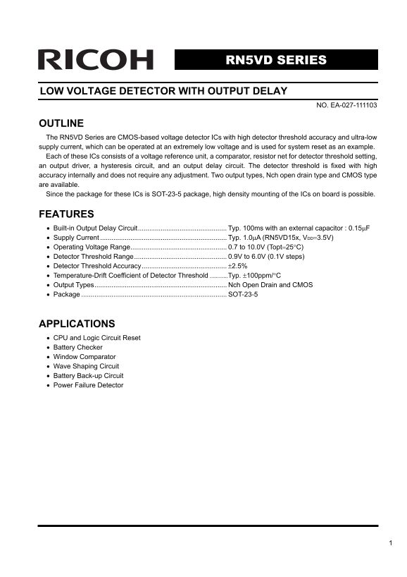
OUTLINE The RN5VD Series are CMOS-based voltage detector ICs with high detector threshold accuracy and ultra-low supply current, which can be operated at an extremely low voltage and is used for system reset as an example. Each of these ICs consists of a voltage reference unit, a comparator, resistor net for detector threshold setting, an output driver, a hysteresis circuit, and an output delay circuit. The detector threshold is fixed with high accuracy internally and does not require any adjustment. Two output types, Nch open drain type and CMOS type are available. Since the package for these ICs is SOT-23-5 package, high density mounting of the ICs on board is possible.

FEATURES • Built-in Output Delay Circuit............................................... Typ. 100ms with an external capacitor : 0.15μF • Supply Current Typ. 1.0μA (RN5VD15x, VDD=3.5V) • Operating Voltage Range................................................... 0.7 to 10.0V (Topt=25°C) • Detector Threshold Range................................................. 0.9V to 6.0V (0.1V steps) • Detector Threshold Accuracy............................................. ±2.5% • Temperature-Drift Coefficient of Detector Threshold ............Typ. ±100ppm/°C • Output Types...................................................................... Nch Open Drain and CMOS • Package SOT-23-5

APPLICATIONS • CPU and Logic Circuit Reset • Battery Checker • Window Comparator • Wave Shaping Circuit • Battery Back-up Circuit • Power Failure Detector

Page Summary Contents For RICOH RN5VD SERIES Owner's Manual User Guide

Page 1 RN5VD SERIES LOW VOLTAGE DETECTOR WITH OUTPUT DELAY NO. EA-027-111103 OUTLINE The RN5VD Series are CMOS-based voltage detector ICs with high detector threshold accuracy and ultra-low supply current, w...
Page 2 RN5VD BLOCK DIAGRAMS RN5VDxx A RN5VDxx C VDD OUT VDD RD RD Vref Vref GND GND CD CD SELECTION GUIDE The detector threshold, and the output type for the ICs can be selected at the users’ request. Produc...
Page 3 RN5VD PIN CONFIGURATION ●SOT-23-5 (mark side) PIN DESCRIPTION Pin No. Symbol Pin Description 1 OUT Output Pin("L" at Detection) 2 VDD Input Pin 3 GND Ground Pin 4 NC No Connection 5 CD Pin f...
Page 4 RN5VD ELECTRICAL CHARACTERISTICS • RN5VD09A/C Topt=25˚C Symbol Item Conditions Min. Typ. Max. Unit. –VDET Detector Threshold 0.878 0.900 0.922 VHYS Detector Threshold Hysteresis 0.027 0.045 0.063 VDD=...
Page 5 RN5VD • RN5VD18A/C Topt=25˚C Symbol Item Conditions Min. Typ. Max. Unit. –VDET Detector Threshold 1.755 1.800 1.845 VHYS Detector Threshold Hysteresis 0.054 0.090 0.126 VDD=1.7V 2.5 5.0 ISS Supply Cur...
Page 6 RN5VD • RN5VD27A/C Topt=25˚C Symbol Item Conditions Min. Typ. Max. Unit. –VDET Detector Threshold 2.633 2.700 2.767 VHYS Detector Threshold Hysteresis 0.081 0.135 0.189 VDD=2.6V 3.5 7.0 ISS Supply Cur...
Page 7 RN5VD • RN5VD36A/C Topt=25˚C Symbol Item Conditions Min. Typ. Max. Unit. –VDET Detector Threshold 3.510 3.600 3.690 VHYS Detector Threshold Hysteresis 0.108 0.180 0.252 VDD=3.47V 4.5 9.0 ISS Supply Cu...
Page 8 RN5VD • RN5VD45A/C Topt=25˚C Symbol Item Conditions Min. Typ. Max. Unit. –VDET Detector Threshold 4.388 4.500 4.612 VHYS Detector Threshold Hysteresis 0.135 0.225 0.315 VDD=4.34V 5.5 11.0 ISS Supply C...
Page 9 RN5VD • RN5VD54A/C Topt=25˚C Symbol Item Conditions Min. Typ. Max. Unit. –VDET Detector Threshold 5.265 5.400 5.535 VHYS Detector Threshold Hysteresis 0.162 0.270 0.378 VDD=5.2V 6.0 12.0 ISS Supply Cu...
Page 10 RN5VD ELECTRICAL CHARACTERISTICS BY DETECTOR THRESHOLD • RN5VD09A/C to RN5VD39A/C Detector Threshold Hysteresis Supply Current 1 Supply Current 2 Output Current 1 Output Current 2 Part Number. –VDET (...
Page 11 RN5VD Topt=25˚C Detector Minimum Oper- CD Pin Output Delay Output Current 3 CD Pin Threshold Voltage CD Pin Output Current 2 Threshold ating Voltage Current 1 Resistance Tempco. ∆–VDET IOUT3 (m A) VDD...
Page 12 RN5VD • RN5VD40A/C to RN5VD60A/C Detector Threshold Hysteresis Supply Current 1 Supply Current 2 Output Current 1 Output Current 2 Part Number. –VDET (V) VHYS (V) Iss1 (µA) Iss2 (µA) IOUT1 (m A) IOUT2...
Page 13 RN5VD Topt=25˚C Detector Minimum Oper- CD Pin Output Delay Output Current 3 CD Pin Threshold Voltage CD Pin Output Current 2 Threshold ating Voltage Current 1 Resistance Tempco. ∆–VDET IOUT3 (m A) VDD...
Page 14 RN5VD OPERATION Ra Current Source Comparator RD Schmitt Trigger Tr.2 Tr.1 Output Capacitor Fig. 1 Block Diagram Step Step 1 Step 2 Step 3 Step 4 Step 5 Comparator (–) Pin II II II Released Voltage +VD...
Page 15 RN5VD • Output Delay Operation Supply Voltage (VDD) Released Voltage (+VDET) CD pin Voltage CD pin Threshold Voltage (VTCD) Output Voltage (OUT) GND Output Delay Time (t D) When the supply voltage cro...
Page 16 RN5VD TEST CIRCUITS +5V or VDD VDD VDD VIN VIN RN5VD RN5VD SERIES SERIES GND GND Fig. 3 Supply Current test Circuit Fig. 4 Detector Threshold Test Circuit VIN IOUT VIN IOUT RN5VD RN5VD××C SERIES SERIE...
Page 17 RN5VD et ec to hr es ho ld (V up pl ur re nt Is s( µA up pl ur re nt Is s( µA TYPICAL CHARACTERISTICS 1) Supply Current vs. Input Voltage RN5VD09x RN5VD27x Topt=80˚C –30˚C Topt=80˚C Input Voltage VIN(...
Page 18 RN5VD ut pu t V ol ta ge (V et ec to hr es ho ld (V ut pu t V ol ta ge (V RN5VD45x +VDET –VDET Temperature Topt(˚C) ut pu t V ol ta ge (V ut pu t V ol ta ge (V 3) Output Voltage vs. Input Voltage VDD ...
Page 19 RN5VD ut pu t C ur re rt IO (m ut pu t C ur re rt IO (m ut pu t V ol ta ge (V VDD Pull-up 5V Pull-up RN5VD45A RN5VD45A Topt= –30˚C Topt= –30˚C 25˚C 80˚C Input Voltage VIN(V) Input Voltage VIN(V) 4) Nc...
Page 20 RN5VD ut pu t C ur re nt IO (m ut pu t C ur re nt IO (m ut pu t C ur re nt IO (m 5) Nch Driver Output Current vs. Input Voltage RN5VD09x RN5VD27x VDS=0.5V VDS=0.5V Topt = –30˚C Topt = 80˚C 0.2 0.4 0.6...
Page 21 RN5VD in hr es ho ld ol ta ge (V in hr es ho ld ol ta ge (V ut pu t C ur re nt IO (m RN5VD45C VDS =–2.1V Input Voltage VIN(V) 7) CD pin Threshold Voltage vs. Temperature in hr es ho ld ol ta ge (V RN5...
Page 22 RN5VD in in ur re nt IC (m in in ur re nt IC (m in in ur re nt IC (m 8) CD pin Sink Current vs. Input Voltage RN5VD09x RN5VD27x VDS=0.5V VDS=0.5V Topt = –30˚C Topt = 80˚C 80˚C 0.2 0.4 0.6 0.8 1.0 0.5 ...
Page 23 RN5VD RN5VD45x ut pu t D el ay im t P (m s) ut pu t D el ay im t P (m s) in in ur re nt IC (m VDD = 4.0V CD pin Voltage VDS(V) 10) Output delay Time vs. External Capacitance RN5VD09A RN5VD27A el ay es...
Page 24 RN5VD TYPICAL APPLICATIONS • RN5VDxx A CPU Reset Circuit (Nch Open Drain Output) (1) Input Voltage to RN5VDxx A is (2) Input Voltage to RN5VDxx A is the same as the input voltage to CPU. different fro...
Page 25 RN5VD • Manual Reset Circuit VDD VDD CD CD RN5VDxx A RN5VDxx C SERIES OUT SERIES OUT CD CD GND GND APPLICATION HINTS VDD VDD RN5VD OUTCD CD RN5VD OUT SERIES SERIES Fig.10 Fig.11 1. When RN5VDxx C (CMO...
Page 26 1. The products and the product specifications described in this document are subject to change or discontinuation of production without notice for reasons such as improvement. Therefore, before decid...

Manual Details

Brand Ricoh
Pages 26
File Size 688.92 KB
Published June 01, 2026
75 views

Enter the captcha to get the download link:

captcha

Frequently Asked Questions

How do I set the delay time for the output signal?

You can set the output delay using an external capacitor connected to Pin 5 (CD). A sample value is 0.15μF for a typical 100ms delay.

What voltage range can be selected as the detector threshold?

The detector threshold can be specified by the user in the range of 0.9V up to 6.0V, utilizing increments of 0.1V.

Which pin is responsible for setting the output delay?

Pin 5 (labeled CD) is dedicated for connecting the external capacitor used to set the detection cycle's output delay.

What is the typical low-voltage power consumption?

The device features a very low typical supply current, such as 1.0μA when operating at VDD=3.5V.