# A B C D E F G H I J K L M N O P Q R S T U V W X Y Z

RICOH R3116x SERIES Low Voltage Detector with Output Delay Data Sheet User Manual

Summary

The R3116x series are high-precision CMOS voltage detector ICs designed for reliable system monitoring and automatic reset functions. These ultra-low power devices detect critical drops in supply voltage across a wide range (0.5V to 6.0V), making them ideal for applications like CPU/logic circuit reset, battery backup systems, and power failure detection. This manual provides comprehensive technical details, including pin configurations, package selection guides, electrical characteristics, and operating limits, enabling engineers to select the precise detector threshold needed for their embedded designs requiring maximum efficiency and reliability.
📄 Preview PAGE OF 24

Page 1 Text Content

R3116x SERIES

0.8% LOW VOLTAGE DETECTOR WITH OUTPUT DELAY

NO.EA-161-120423

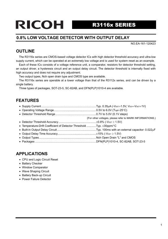
OUTLINE The R3116x series are CMOS-based voltage detector ICs with high detector threshold accuracy and ultra-low supply current, which can be operated at an extremely low voltage and is used for system reset as an example. Each of these ICs consists of a voltage reference unit, a comparator, resistors for detector threshold setting, an output driver, a hysteresis circuit and an output delay circuit. The detector threshold is internally fixed with high accuracy and does not require any adjustment. Two output types, Nch open drain type and CMOS type are available. The R3116x series are operable at a lower voltage than that of the R3112x series, and can be driven by a single battery. Three types of packages, SOT-23-5, SC-82AB, and DFN(PLP)1010-4 are available.

FEATURES • Supply Current ......................................................................Typ. 0.35μA (-VDET=1.5V, VDD=-VDET+1V) • Operating Voltage Range......................................................0.5V to 6.0V (Topt=25°C) • Detector Threshold Range....................................................0.7V to 5.0V (0.1V steps) (For other voltages, please refer to MARK INFORMATIONS.) • Detector Threshold Accuracy................................................±0.8% (-VDET ≥ 1.5V) • Temperature-Drift Coefficient of Detector Threshold ............Typ. ±30ppm/°C • Built-in Output Delay Circuit..................................................Typ. 100ms with an external capacitor: 0.022μF • Output Delay Time Accuracy.................................................±15% (-VDET ≥ 1.5V) • Output Types.........................................................................Nch Open Drain "L" and CMOS • Packages ..............................................................................DFN(PLP)1010-4, SC-82AB, SOT-23-5

APPLICATIONS • CPU and Logic Circuit Reset • Battery Checker • Window Comparator • Wave Shaping Circuit • Battery Back-up Circuit • Power Failure Detector

Page Summary Contents For RICOH R3116x SERIES Low Voltage Detector with Output Delay Data Sheet User Manual

Page 1 R3116x SERIES 0.8% LOW VOLTAGE DETECTOR WITH OUTPUT DELAY NO.EA-161-120423 OUTLINE The R3116x series are CMOS-based voltage detector ICs with high detector threshold accuracy and ultra-low supply curr...
Page 2 BLOCK DIAGRAMS Nch Open Drain Output (R3116xxx1A) CMOS Output (R3116xxx1C) OUTVDD VDD Delay Delay Circuit Circuit Vref Vref GND GND CD CD SELECTION GUIDE The package type, the detector threshold, the ...
Page 3 PIN CONFIGURATIONS • DFN(PLP)1010-4∗ Top View Bottom View • SOT-23-5 • SC-82AB (mark side) (mark side) PIN DESCRIPTIONS • DFN(PLP)1010-4∗ • SOT-23-5 Pin No. Symbol Description Pin No. Symbol Descripti...
Page 4 ABSOLUTE MAXIMUM RATINGS Symbol Item Rating Unit VDD Supply Voltage 7.0 V Output Voltage (Nch Open Drain Output) VSS−0.3 to 7.0 Output Voltage (CMOS Output) VSS−0.3 to VDD+0.3 IOUT Output Current 20 m...
Page 5 ELECTRICAL CHARACTERISTICS • R3116xxx1A/C values indicate −40°C ≤ Topt ≤ 85°C, unless otherwise noted. Topt=25°C Symbol Item Conditions Min. Typ. Max. Unit 1.5V < -VDET ≤ 5.0V -VDET Topt=25°C × 0.9...
Page 6 TIMING CHART When the supply voltage, which is higher than released voltage, is forced to VDD pin, charge to an external capacitor starts, then CD pin voltage increases. Until the CD pin voltage reach...
Page 7 ELECTRICAL CHARACTERISTICS BY DETECTOR THRESHOLD • R3116x071A/C to R3116x501A/C Bold values are checked and guaranteed by design engineering at −40°C ≤ Topt ≤ 85°C, unless otherwise noted. Topt=25°C D...
Page 8 Detector Threshold Nch Driver Output Nch Driver Output Pch Driver Output Nch Driver Output Delay Temperature Current1 Current2 Current Leakage Current Time Coefficient IOUT1 [µA] IOUT2 [m A] IOUT3 [m ...
Page 9 OPERATION • Operation of R3116xxx1A Comparator Delay OUT pin should be pulled-up to Circuit VDD or an external voltage level. Rb Vref Nch Block Diagram (R3116xxx1A) Step 1 2 3 4 Released Voltage +VDET...
Page 10 • Operation of R3116xxx1C Comparator Ra Pch Delay Circuit Rb Vref Nch Block Diagram (R3116xxx1C) Step 1 2 3 4 Released Voltage +VDET Comparator (−) A BDetector Threshold Hysteresis II II II Detector T...
Page 11 ls id th μs R3116x Detector Operation vs. glitch input voltage to the VDD pin When the R3116x is at released, if the pulse voltage which the detector threshold or lower voltage, the graph below means ...
Page 12 TEST CIRCUITS 5V or VDD VDD VDD VIN VIN Series Series GND GND Supply Current Test Circuit Detector Threshold Test Circuit (Pull-up circuit is not necessary for CMOS Output type.) VDD VDD VDS IOUT IOUT...
Page 13 te to re ld /R le lt ly rr IS μA ly rr IS μA TYPICAL CHARACTERISTICS 1) Supply Current vs. Input Voltage R3116x071A/C R3116x151A/C 1.0 1.0 Topt=85°C Topt=85°C Topt=25°C Topt=25°C Topt=- 40°C Topt=- 40...
Page 14 te to re ld /R le lt tp lt tp lt +VDET 2.85 4.8 +VDET -VDET -VDET Temperature Topt (°C) Temperature Topt (°C) te to re ld /R le lt tp lt tp lt 3) Output Voltage vs. Input Voltage Topt=- 40°C Topt=- 40...
Page 15 ri tp rr IO tp lt tp lt 470kΩ 5V Pull-Up 470kΩ 5V Pull-Up Topt=- 40°C Topt=- 40°C Topt=25°C Topt=25°C Topt=85°C Topt=85°C Input Voltage VDD (V) Input Voltage VDD (V) ri tp rr IO tp lt tp lt 470kΩ 5V P...
Page 16 ri tp rr IO ri tp rr IO ri tp rr IO Topt=- 40°C Topt=- 40°C Topt=25°C 6.0 Topt=25°C Topt=85°C Topt=85°C Input Voltage VDD (V) Input Voltage VDD (V) ri tp rr IO ri tp rr IO ri tp rr IO 5) Nch Driver Ou...
Page 17 ri tp rr IO ri tp rr IO ri tp rr IO 6) Pch Driver Output Current vs. Input Voltage (VDS=−2.1V) Topt=- 40°C Topt=- 40°C Topt=25°C Topt=25°C Topt=85°C Topt=85°C Input Voltage VDD (V) Input Voltage VDD (...
Page 18 la im /t la im /t ri tp rr IO VDD=6.0V VDD=6.0V VDD=5.0V VDD=5.0V 2.0 VDD=4.0V 2.0 VDD=3.0V VDS (V) VDS (V) la im /t la im /t ri tp rr IO 8) Output Delay Time vs. External Capacitance t PHL t PHL Exte...
Page 19 tp la im tp la im 9) Output Delay Time vs. Temperature (CD=22n F) Temperature Topt (°C) Temperature Topt (°C) tp la im tp la im Temperature Topt (°C) Temperature Topt (°C)
Page 20 TYPICAL APPLICATION • R3116xxx1A CPU Reset Circuit 1 (Nch Open Drain Output) Case1. Input Voltage to R3116xxx1A is equal to Case2. Input Voltage to R3116xxx1A is unequal to Input Voltage to CPU Input ...
Page 21 • Voltage level Indicator Circuit (lighted when the power runs out) (Nch Open Drain Output) R3116xxx1A Series CD OUT • Detector Threshold Adjustable Circuit 1 (Nch Open Drain Output) Adjustable Detect...
Page 22 • Window Comparator Circuit (Nch Open Drain Output) VDD VDD −VDET1 −VDET2 Rup1 Rup2 CD R3116xxx1A OUT WC_OUT So la r B at te ry D1 Series VDD −VDET2 R3116xxx1A OUT Series CD −VDET1 WC_OUT • Over-charg...
Page 23 TECHNICAL NOTES When R3116xxx1A/C is used in Figure X, if the value of R1 is set excessively large, the dropdown voltage caused by the consumption current of IC itself, may vary the detector threshold...
Page 24 1. The products and the product specifications described in this document are subject to change or discontinuation of production without notice for reasons such as improvement. Therefore, before decid...

Manual Details

Brand Ricoh
Pages 24
File Size 445.33 KB
Published May 27, 2026
80 views

Enter the captcha to get the download link:

captcha

Frequently Asked Questions

What is the typical supply current for the R3116x series?

The typical supply current is 0.35μA (assuming VDET=1.5V, VDD=-VDET+1V).

Can this voltage detector be powered by a single battery?

Yes, the R3116x series are operable at lower voltages than the R3112x series and can be driven by a single battery.

What types of output signals are available?

Two output types are available: Nch Open Drain "L" and CMOS type

How is the detector threshold set or adjusted?

The detector threshold is internally fixed with high accuracy (±0.8%) and does not require any adjustment.