# A B C D E F G H I J K L M N O P Q R S T U V W X Y Z

RICOH R3118x SERIES LOW VOLTAGE DETECTOR with individual SENSE pin and delay function

Summary

The R3118x series are high-accuracy, CMOS voltage detector ICs essential for maintaining system stability and detecting undervoltage conditions. This manual details these sophisticated supervisors, which utilize separate power and sense pins to ensure reliable output signaling even upon detecting low voltages. Featuring adjustable reset delays and highly precise detection thresholds (0.6V to 5.0V), this product is ideal for embedded electronics engineers designing critical applications such as CPU/logic circuit resets, battery backup systems, or power failure detection circuits needing maximum reliability and minimal current consumption.
📄 Preview PAGE OF 23

Page 1 Text Content

R3118x SERIES

LOW VOLTAGE DETECTOR with individual SENSE pin and delay function

NO.EA-242-111104

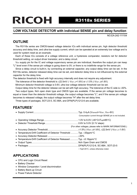
OUTLINE The R3118x series are CMOS-based voltage detector ICs with individual sense pin, high detector threshold accuracy and delay time, and ultra-low supply current, which can be operated at an extremely low voltage and is used for system reset as an example. Each of these ICs consists of a voltage reference unit, a hysteresis comparator, resistors net for detector threshold setting, an output driver transistor, and a delay circuit. VDD supply pin for the IC and voltage supervisory sense pin are individual, therefore the output pin can keep "L" level even if the sense pin voltage is going down to 0V, or there is no indefinite range for the sense pin. Since a delay circuit is built-in, by connecting an external capacitor, any output delay time can be set. In the R3118x series, detector released delay time can be set, and detector delay time is not influenced by the external capacitor for the delay time. The detector threshold is fixed with high accuracy internally and does not require any adjustment. The tolerance of the detector threshold is ±22.5m V (−VDET_S<1.6V) or ±1.5% (-VDET_S≥1.6V). Minimum detector threshold voltage is 0.6V, ultra low voltage detector threshold can be set. Output delay time for the detector release can be set with high accuracy. The tolerance of the IC side is ±30%. Two output types, Nch open drain type and CMOS type are available. If the sense pin voltage becomes to equal or lower than the detector threshold voltage, the output voltage becomes "L", and if the sense pin voltage becomes to released voltage, the output voltage becomes "H" after the set delay time. Three types of packages, SOT-23-5, SC-88A, and DFN(PLP)1212-6 are available.

FEATURES∗ • Supply Current ......................................................................Typ. 0.4μA (VSENSE≥+VDET, VDD=6V)

Consumption current through SENSE pin is not included.

• Operating Voltage Range......................................................1.0V to 6.0V (-40°C≤Topt≤85°C) • Detector Threshold Range....................................................0.6V to 5.0V (0.1V steps) (For other voltages, please refer to MARK INFORMATIONS.) • Accuracy Detector Threshold................................................±1.5% (-VDET_S≥1.6V), ±22.5m V (-VDET_S<1.6V) • Temperature-Drift Coefficient of Detector Threshold ............Typ. ±30ppm/°C • Accuracy Detector Released ................................................±30% • Temperature-Drift Coefficient of Detector Released .............Typ. ±0.16ppm/°C • Output Types.........................................................................Nch Open Drain and CMOS • Packages ..............................................................................DFN(PLP)1212-6, SC-88A , SOT-23-5

∗ Topt=25°C, unless otherwise noted.

APPLICATIONS • CPU and Logic Circuit Reset • Battery Checker • Window Comparator / Level discrimination • Battery Back-up Circuit • Power Failure Detector

Page Summary Contents For RICOH R3118x SERIES LOW VOLTAGE DETECTOR with individual SENSE pin and delay function

Page 1 R3118x SERIES LOW VOLTAGE DETECTOR with individual SENSE pin and delay function NO.EA-242-111104 OUTLINE The R3118x series are CMOS-based voltage detector ICs with individual sense pin, high detector ...
Page 2 BLOCK DIAGRAMS Nch Open Drain Output (R3118xxxx A) CMOS Output (R3118xxxx C) SENSE SENSE DOUTVDD VDD Delay Delay Circuit Circuit Vref Vref GND GND CD CD SELECTION GUIDE The package type, the detector ...
Page 3 PIN CONFIGURATIONS • DFN(PLP)1212-6 • SC-88A • SOT-23-5 Top View Bottom View (mark side) (mark side) PIN DESCRIPTIONS • DFN(PLP)1212-6 • SC-88A Pin No. Symbol Description Pin No. Symbol Description 1 ...
Page 4 ABSOLUTE MAXIMUM RATINGS Symbol Item Rating Unit VDD Supply Voltage −0.3 to 7.0 V VSENSE SENSE Pin Voltage −0.3 to 7.0 V Output Voltage (Nch Open Drain Output) −0.3 to 7.0 VDOUT Output Voltage (CMOS O...
Page 5 Symbol Item Conditions Min. Typ. Max. Unit VSENSE=0V, VDD=6V 0.480 1.450 ISS Supply Current *1 μA VSENSE=6V, VDD=6V 0.400 1.200 RSENSE Sense Resistor VSENSE=6V, VDD=6V 9 34 58 MΩ VDD=1V, VDOUT=0.1V 0....
Page 6 TIMING CHART Supply Voltage (VDD) Minimum Operating VDDL Voltage Detector Threshold Detector Threshold Hysteresis Hysteresis Released Voltage +VDET Detector Threshold -VDET SENSE Pin Voltage (VSENSE) ...
Page 7 DEFINITION OF OUTPUT DELAY TIME A higher voltage than the released voltage is forced to the SENSE pin, charge to the capacitor connected to CD pin is started, then the CD pin voltage increases. Until ...
Page 8 OPERATION • Operation of R3118xxxx A SENSE Comparator ∗)DOUT pin should be pulled-up to VDD or an external voltage level. Delay DOUT Circuit Tr.1 Nch Block diagram with an external capacitor (R3118xxx...
Page 9 • Operation of R3118xxxx C SENSE Comparator Delay Circuit Tr.1 Nch Block diagram with an external capacitor (R3118xxxx C) Supply Voltage (VDD) Minimum Operating Step 1 2 3 Voltage Comparator (−) Pin I...
Page 10 • In case of the SENSE pin voltage is forced after the VDD pin voltage is forced. VDD pin voltage VDD Time t SENSE pin voltage VSENSE Released Voltage +VDET Detector Threshold -VDET Time t DOUT pin vo...
Page 11 • In case of the VDD pin voltage is forced after the SENSE pin voltage is forced. VDD pin voltage VDD Time t SENSE pin voltage VSENSE Released Voltage +VDET Detector Threshold -VDET Time t DOUT pin vo...
Page 12 TYPICAL APPLICATION • R3118xxxx A CPU Reset Circuit (Nch Open Drain Output) (1) VDD pin Voltage to R3118xxxx A is equal to VDD pin Voltage to CPU VDD VDD SENSE R3118xxxx A Series DOUT RESET GND CD GND...
Page 13 TEST CIRCUITS VDD VDD SENSE SENSE 470kΩ R3118x R3118x DOUT DOUT Series Series GND CD GND CD Supply Current Test Circuit Detector Threshold Test Circuit (Pull-up circuit is not necessary for CMOS Outpu...
Page 14 et ec to r T hr es ho ld T ( et ec to r T hr es ho ld Su pp ly ur re nt S ( μA TYPICAL CHARACTERISTICS 1) Supply Current vs. Supply Voltage R3118xxxx A/C (VSENSE=0V) R3118xxxx A/C (VSENSE=6V) 1.0 1.0 ...
Page 15 et ec to r T hr es ho ld et ec to r T hr es ho ld T ( et ec to r T hr es ho ld T ( ys te re si S ( 3) Detector Threshold vs. Supply Voltage Topt=-40°C Topt=-40°C 0.606 Topt=25°C 2.727 Topt=25°C Topt=8...
Page 16 et ec to r T hr es ho ld et ec to r T hr es ho ld et ec to r T hr es ho ld ys te re si S ( ys te re si S ( R3118x ys te re si S ( R3118x50x A/C (VDD=5.3V) Temperature Topt (°C) et ec to r T hr es ho l...
Page 17 ch riv er ut pu t C ur re nt ut pu t V ol ta ge (V ut pu t V ol ta ge (V 6) Output Voltage vs. SENSE Voltage (DOUT pin is pulled up to VDD pin via 470kΩ.) R3118x06x A/C R3118x27x A/C VDD=1V VDD=3V VDD...
Page 18 in is ch ar ge r O in is ch ar ge r. Pc riv er ut pu t C ur re nt R3118x es is to r R IS (k hm es is to r R (k hm IS (μ A) 9) Pch Driver Output Current vs. Supply Voltage 10) Pch Driver Output current...
Page 19 el ea se et ec el ea se el ay im de la y ( s) R3118x el ea se el ay im el ay im de la y / re se t ( s) de la y ( s) 13) Release Output Delay Time vs. Temperature R3118xxxx A/C (VDD=4V, CD=0.022μF) -50...
Page 20 et ec t D el ay im re se t ( μs 16) Detect Output Delay time vs. Over-drive Voltage SENSE pin Voltage VSENSE Detector Threshold (-VDET) Over-drive Voltage (VOD) Time t DOUT pin Voltage VDOUT et ec t D...
Page 21 el ea se el ay im de la y ( μs R3118x 17) Release Output Delay time vs. Over-drive Voltage SENSE pin Voltage VSENSE Over-drive Voltage (VOD) Released Voltage (+VDET) Time t DOUT pin Voltage VDOUT Rele...
Page 22 TECHNICAL NOTES When R3118xxxx A/C is used in the circuit as SENSE pin and VDD pin are connected each other such as in Fig. A, if the value of R1 is set excessively large, the dropdown voltage caused ...
Page 23 1. The products and the product specifications described in this document are subject to change or discontinuation of production without notice for reasons such as improvement. Therefore, before decid...

Manual Details

Brand Ricoh
Pages 23
File Size 482.36 KB
Published May 27, 2026
84 views

Enter the captcha to get the download link:

captcha

Frequently Asked Questions

How do I set the output delay time?

The output delay can be set by connecting an external capacitor to the designated pins.

What is the typical supply current consumption of this IC?

The typical supply current is 0.4μA, provided that V_SENSE $\geq$ +VDET and VDD=6V (sense pin consumption excluded).

Why are the VDD supply pin and voltage supervisory sense pin individual?

This design ensures the output pin remains in an "L" level even if the sense pin drops down to 0V or has no indefinite range.