National Semiconductor MM54C157 MM74C157 Quad 2-Input Multiplexers Data Sheet Manual
Summary
This highly reliable Quad 2-Input Multiplexer is a low-power CMOS integrated circuit ideal for digital signal switching applications. Featuring four independent multiplexing channels with common select and enable inputs, it ensures high noise immunity and excellent TTL compatibility across operational voltages (3V to 15V). The accompanying manual provides comprehensive engineering data, including detailed electrical characteristics, absolute maximum ratings, timing specifications, and various package options necessary for accurate circuit board design.
Page 1 Text Content
查询MM54C157供应商
February
-In ltip le rs
MM54C157/MM74C157 Quad 2-Input Multiplexers General Description Features
These multiplexers are monolithic complementary MOS Supply voltage range 3V to 15V
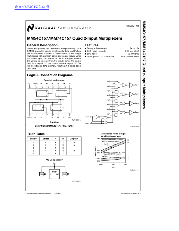
(CMOS) integrated circuits constructed with N- and P-chan- High noise immunity 0.45 VCC (typ.) nel enhancement transistors. They consist of four 2-input Low power n W (typ.) multiplexers with common select and enable inputs. When Tenth power TTL compatible Drive LPTTL loads the enable input is at logical ‘‘0’’ the four outputs assume the values as selected from the inputs. When the enable input is at logical ‘‘1’’, the outputs assume logical ‘‘0’’. Se- lect decoding is done internally resulting in single select input only.
Logic Connection Diagrams
Dual-In-Line Package
TL/F/5894–2
Order Number MM54C157 or MM74C157 TL/F/5894–1
Truth Table Guaranteed Noise Margin as Function of VCC
Enable Select Output
74L Compatibility
TL/F/5894–4
TL/F/5894–3
C1995 National Semiconductor Corporation TL/F/5894 RRD-B30M105/Printed in U. S. A.
Page Summary Contents For National Semiconductor MM54C157 MM74C157 Quad 2-Input Multiplexers Data Sheet Manual
Manual Details
| Brand | National |
|---|---|
| Pages | 4 |
| File Size | 100.86 KB |
| Published | June 16, 2026 |
Enter the captcha to get the download link:

Frequently Asked Questions
What is the operating voltage range for this device?
The recommended supply voltage range is 3V to 15V.
How does the multiplexer output behave when the enable input is low (logical '0')?
If the enable input is low, all four outputs assume logical '0'.
What different packages are available for this component?
Available packages include Dual-In-Line Package (J) and Molded Dual-In-Line Package (N).
Can this device be used in life support systems?
No, National Semiconductor states that these products are not authorized for use as critical components in life support devices.