Motorola MPC2002 MPC2003 User Guide
Summary
Engineers seeking high-speed memory solutions for PowerPC 60x processors must use the MPC2002/MPC2003 Fast SRAM Cache Modules. These highly reliable, burstable DIMM modules provide essential L2 cache capacity (256K/512K) for critical system performance. This manual is a comprehensive technical datasheet, providing detailed operational specifications, pin assignments, electrical block diagrams, and interface guidelines. It serves professionals designing embedded systems that require rock-solid memory integration within PowerPC architecture platforms.
Page 1 Text Content
查询MPC2002供应商
Order this document
SEMICONDUCTOR TECHNICAL DATA by MPC2002/D
MPC2002
256KB and 512KB Burst RAM
MPC2003
Secondary Cache Module for
(Formerly MCM72MS32/64)
Power PC – Based Systems
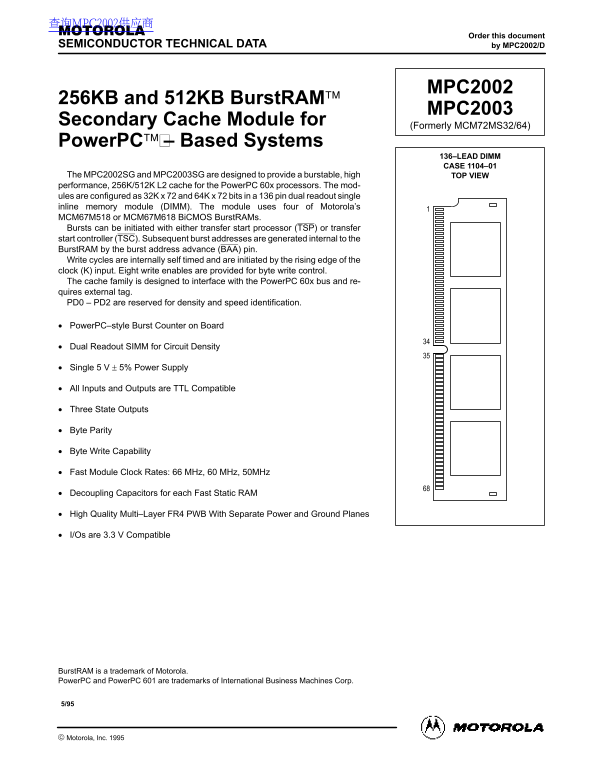
136–LEAD DIMM CASE 1104–01
The MPC2002SG and MPC2003SG are designed to provide a burstable, high TOP VIEW performance, 256K/512K L2 cache for the Power PC 60x processors. The mod- ules are configured as 32K x 72 and 64K x 72 bits in a 136 pin dual readout single inline memory module (DIMM). The module uses four of Motorola’s MCM67M518 or MCM67M618 Bi CMOS Burst RAMs. Bursts can be initiated with either transfer start processor (TSP) or transfer start controller (TSC). Subsequent burst addresses are generated internal to the Burst RAM by the burst address advance (BAA) pin. Write cycles are internally self timed and are initiated by the rising edge of the clock (K) input. Eight write enables are provided for byte write control. The cache family is designed to interface with the Power PC 60x bus and re- quires external tag. PD0 – PD2 are reserved for density and speed identification.
Power PC–style Burst Counter on Board
Dual Readout SIMM for Circuit Density
Single 5 V ± 5% Power Supply
All Inputs and Outputs are TTL Compatible
Three State Outputs
Byte Parity
Byte Write Capability
Fast Module Clock Rates: 66 MHz, 60 MHz, 50MHz
Decoupling Capacitors for each Fast Static RAM
High Quality Multi–Layer FR4 PWB With Separate Power and Ground Planes
I/Os are 3.3 V Compatible
Burst RAM is a trademark of Motorola. Power PC and Power PC 601 are trademarks of International Business Machines Corp.
MOTOROLA FAST SRAM Motorola, Inc. 1995 MPC2002•MPC2003
Page Summary Contents For Motorola MPC2002 MPC2003 User Guide
Manual Details
| Brand | Motorola |
|---|---|
| Pages | 14 |
| File Size | 238.62 KB |
| Published | June 01, 2026 |
Enter the captcha to get the download link:

Frequently Asked Questions
What type of processor bus is this SRAM designed to interface with?
The cache family is designed specifically to interface with the PowerPC 60x bus.
How are bursts initiated on this module?
Bursts can be initiated using either a transfer start processor (TSP) or a transfer start controller (TSC).
What operating speeds are supported by these modules?
The fast module clock rates include 66 MHz, 60 MHz, and 50 MHz.
Can this product be used in life-support systems or surgical implants?
No. The manual explicitly forbids use in systems intended for surgical implant into the body, or applications that support or sustain life.