MOTOROLA MCM64PD32 MCM64PD64 User Guide and Manual
Summary
Boost system performance significantly with these MCM64PD cache modules, designed as high-speed L2 secondary caches for Pentium microprocessors leveraging Intel's Triton II chipset. This detailed manual provides comprehensive technical data, including block diagrams, pin assignments, and functional specifications for both 256K and 512K versions. It is essential reading for hardware engineers and system designers integrating burstable SRAM into complex computer architectures requiring high-speed memory interfacing.
Page 1 Text Content
Order this document
SEMICONDUCTOR TECHNICAL DATA by MCM64PD32/D
MCM64PD32
Advance Information
MCM64PD64
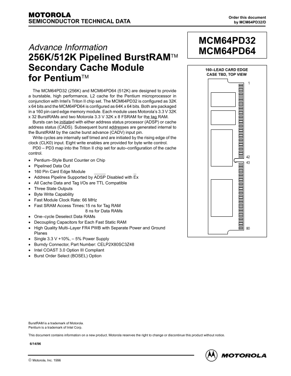
256K/512K Pipelined Burst RAM Secondary Cache Module 160–LEAD CARD EDGE
CASE TBD, TOP VIEW
for Pentium The MCM64PD32 (256K) and MCM64PD64 (512K) are designed to provide a burstable, high performance, L2 cache for the Pentium microprocessor in conjunction with Intel’s Triton II chip set. The MCM64PD32 is configured as 32K x 64 bits and the MCM64PD64 is configured as 64K x 64 bits. Both are packaged in a 160 pin card edge memory module. Each module uses Motorola’s 3.3 V 32K x 32 Burst RAMs and two Motorola 3.3 V 32K x 8 FSRAM for the tag RAM. Bursts can be initiated with either address status processor (ADSP) or cache address status (CADS). Subsequent burst addresses are generated internal to the Burst RAM by the cache burst advance (CADV) input pin. Write cycles are internally self timed and are initiated by the rising edge of the clock (CLK0) input. Eight write enables are provided for byte write control. PD0 – PD3 map into the Triton II chip set for auto–configuration of the cache control. Pentium–Style Burst Counter on Chip Pipelined Data Out 160 Pin Card Edge Module Address Pipeline Supported by ADSP Disabled with Ex All Cache Data and Tag I/Os are TTL Compatible Three State Outputs Byte Write Capability Fast Module Clock Rate: 66 MHz Fast SRAM Access Times:15 ns for Tag RAM
8 ns for Data RAMs
One–cycle Deselect Data RAMs Decoupling Capacitors for Each Fast Static RAM High Quality Multi–Layer FR4 PWB with Separate Power and Ground Planes Single 3.3 V +10%, – 5% Power Supply Burndy Connector, Part Number: CELP2X80SC3Z48 Intel COAST 3.0 Option III Compliant Burst Order Select (BOSEL) Option
Burst RAM is a trademark of Motorola. Pentium is a trademark of Intel Corp.
This document contains information on a new product. Motorola reserves the right to change or discontinue this product without notice.
MOTOROLA FAST SRAM Motorola, Inc. 1996 MCM64PD32•MCM64PD64
Page Summary Contents For MOTOROLA MCM64PD32 MCM64PD64 User Guide and Manual
Manual Details
| Brand | Motorola |
|---|---|
| Pages | 16 |
| File Size | 184.00 KB |
| Published | June 06, 2026 |
Enter the captcha to get the download link:

Frequently Asked Questions
What microprocessors and chip sets are compatible with this module?
It was designed for the Pentium microprocessor in conjunction with Intel’s Triton II chip set.
What is the speed of the data modules?
The fast module clock rate is 66 MHz, and Data RAM access times are specified at 8 ns.
Does this device support granular write control?
Yes, it includes byte write capability, utilizing eight provided write enables for precise control.
Are there safety restrictions regarding its use?
It must not be used in life-support systems or applications involving surgical implants due to risk of personal injury.