MOTOROLA MC10EL34 MC100EL34 User Guide and Owner's Manual (Part 1)
Summary
Achieve highly stable clock timing with this low skew clock generation chip. Designed for complex digital systems requiring precise signal distribution, the device offers synchronous dividers (÷2, ÷4, ÷8) and supports various differential/single-ended input standards. This manual provides comprehensive technical documentation, including functional tables, detailed electrical characteristics, synchronization methods, and advanced timing diagrams. Ideal for engineers developing high-speed electronic systems who need reliable, low-jitter clock signals from a single source.
Page 1 Text Content
SEMICONDUCTOR TECHNICAL DATA
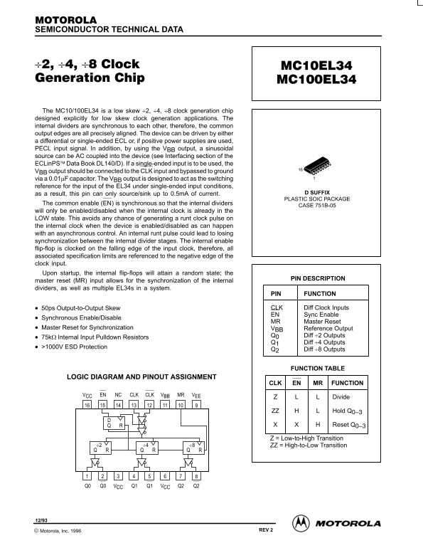
The MC10/100EL34 is a low skew ÷2, ÷4, ÷8 clock generation chip designed explicitly for low skew clock generation applications. The internal dividers are synchronous to each other, therefore, the common output edges are all precisely aligned. The device can be driven by either a differential or single-ended ECL or, if positive power supplies are used, PECL input signal. In addition, by using the VBB output, a sinusoidal source can be AC coupled into the device (see Interfacing section of the ECLin PS Data Book DL140/D). If a single-ended input is to be used, the VBB output should be connected to the CLK input and bypassed to ground via a 0.01µF capacitor. The VBB output is designed to act as the switching reference for the input of the EL34 under single-ended input conditions,
as a result, this pin can only source/sink up to 0.5m A of current. D SUFFIX PLASTIC SOIC PACKAGE
The common enable (EN) is synchronous so that the internal dividers
CASE 751B-05
will only be enabled/disabled when the internal clock is already in the LOW state. This avoids any chance of generating a runt clock pulse on the internal clock when the device is enabled/disabled as can happen with an asynchronous control. An internal runt pulse could lead to losing synchronization between the internal divider stages. The internal enable flip-flop is clocked on the falling edge of the input clock, therefore, all associated specification limits are referenced to the negative edge of the clock input. Upon startup, the internal flip-flops will attain a random state; the
PIN DESCRIPTION
master reset (MR) input allows for the synchronization of the internal dividers, as well as multiple EL34s in a system.
PIN FUNCTION
50ps Output-to-Output Skew CLK Diff Clock Inputs
EN Sync Enable
Synchronous Enable/Disable
MR Master Reset
Master Reset for Synchronization VBB Reference Output
Q0 Diff ÷2 Outputs
75kΩ Internal Input Pulldown Resistors
Q1 Diff ÷4 Outputs
>1000V ESD Protection
Q2 Diff ÷8 Outputs
FUNCTION TABLE
LOGIC DIAGRAM AND PINOUT ASSIGNMENT
CLK EN MR FUNCTION
VCC EN NC CLK CLK VBB MR VEE
Divide
ZZ Hold Q0–3
Reset Q0–3
Z = Low-to-High Transition
÷2 ÷4 ÷8 ZZ = High-to-Low Transition
Q0 VCC Q1 Q1 VCC Q2Q0 Q2
3–1 REV 2 Motorola, Inc. 1996
Page Summary Contents For MOTOROLA MC10EL34 MC100EL34 User Guide and Owner's Manual (Part 1)
Manual Details
| Brand | Motorola |
|---|---|
| Pages | 4 |
| File Size | 62.18 KB |
| Published | May 31, 2026 |
Enter the captcha to get the download link:

Frequently Asked Questions
What does 'low skew' mean for the MC10EL34?
The chips generate low skew clocks because their internal dividers are synchronous, ensuring common output edges are precisely aligned.
How should I handle single-ended input conditions?
Connect the 16V output to the CLK input and bypass it to ground BB 1 using a 0.01μF capacitor.
What does the EN pin do regarding synchronization?
The EN signal must be synchronous, meaning the dividers only enable/disable when the internal clock is already in the LOW state, preventing runt pulses.
How can I synchronize multiple EL34 chips in a system?
Use the Master Reset (MR) input pin to allow for synchronization of the internal dividers across multiple EL34 devices.