MOTOROLA MC10E416 MC100E416 User Guide and Owner's Manual (Part 1)
Summary
The MC10E416/MC100E416 is a high-speed, 5-bit differential line receiving device designed for robust signal buffering and high-bandwidth amplifier applications. Featuring internal gain stages and up to 2.0GHz bandwidth, the component is excellent for handling very fast oscillators in demanding electronic systems. This manual serves as an essential technical resource, providing comprehensive data on electrical specifications, operational limits (DC/AC), pin functionality, and physical package details for system designers integrating high-performance signal conditioning into their designs.
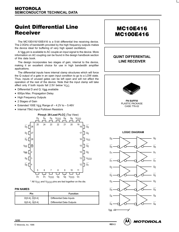
Page 1 Text Content
SEMICONDUCTOR TECHNICAL DATA
The MC10E416/100E416 is a 5-bit differential line receiving device. The 2.0GHz of bandwidth provided by the high frequency outputs makes the device ideal for buffering of very high speed oscillators. A VBB pin is available to AC couple an input signal to the device. More information on AC coupling can be found in the design handbook section
QUINT DIFFERENTIAL
of this data book.
The design incorporates two stages of gain, internal to the device, LINE RECEIVER
making it an excellent choice for use in high bandwidth amplifier applications. The differential inputs have internal clamp structures which will force the Q output of a gate in an open input condition to go to a LOW state. Thus, inputs of unused gates can be left open and will not affect the operation of the rest of the device. Note that the input clamp will take affect only if both inputs fall 2.5V below VCC. Differential D and Q; VBB available 600ps Max. Propagation Delay High Frequency Outputs
2 Stages of Gain FN SUFFIX PLASTIC PACKAGE
Extended 100E VEE Range of – 4.2V to – 5.46V
CASE 776-02
Internal 75kΩ Input Pulldown Resistors
Pinout: 28-Lead PLCC (Top View) D3 D4 D4 VCCO Q4 Q4 VCCO
LOGIC DIAGRAM
D2 VCC
VEE Q2
VBB Q2 D1 Q1
D0 VCCO
D1 D1 VCCO Q0 Q0 VCCO Q1
* All VCC and VCCO pins are tied together on the die. D3 Q3
PIN NAMES D3 Q3
Pin Function
D[0:4], D[0:4] Differential Data Inputs Q[0:4], Q[0:4] Differential Data Outputs
2–1 REV 2 Motorola, Inc. 1996
Page Summary Contents For MOTOROLA MC10E416 MC100E416 User Guide and Owner's Manual (Part 1)
Manual Details
| Brand | Motorola |
|---|---|
| Pages | 5 |
| File Size | 68.50 KB |
| Published | May 30, 2026 |
Enter the captcha to get the download link:

Frequently Asked Questions
What is the maximum propagation delay?
The typical propagation delay (PLH) for both MC10E and MC100E at 25°C is 350 ps.
Can I AC couple an input signal to this device?
Yes, a V pin is available specifically for AC coupling of the input signal to the device.
What are the operating voltage ranges?
The MC10E provides a range of –4.2V to –5.46V, while the MC100E uses an extended range also specified in the data.
How does unused input affect the circuit operation?
Differential inputs have internal clamp structures which ensure that unused gates remain at a LOW state and do not affect operation.