Motorola MC100LVEL29 MC100EL29 User Guide (1)
Summary
This comprehensive datasheet provides the technical specifications for the MC100LVEL29 dual master–slave flip-flop. Designed for high-speed digital logic, this component features fully differential inputs and outputs utilizing specialized ECL signaling levels. The manual details critical operational parameters, including truth tables, setup/hold times, maximum toggle frequency up to 1.1 GHz, and performance across extreme temperature ranges. It is essential documentation for hardware engineers and circuit designers building reliable, high-speed digital systems requiring precise control and robust timing accuracy.
Page 1 Text Content
SEMICONDUCTOR TECHNICAL DATA
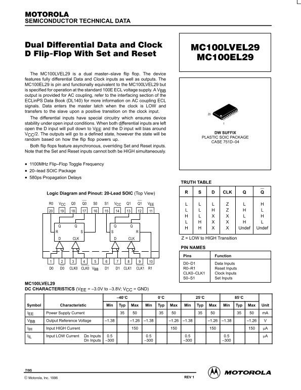
The MC100LVEL29 is a dual master–slave flip flop. The device features fully differential Data and Clock inputs as well as outputs. The MC100EL29 is pin and functionally equivalent to the MC100LVEL29 but is specified for operation at the standard 100E ECL voltage supply. A VBB output is provided for AC coupling, refer to the interfacing section of the ECLin PS Data Book (DL140) for more information on AC coupling ECL signals. Data enters the master latch when the clock is LOW and transfers to the slave upon a positive transition on the clock input. The differential inputs have special circuitry which ensures device stability under open input conditions. When both differential inputs are left open the D input will pull down to VEE and the D input will bias around
DW SUFFIX
VCC/2. The outputs will go to a defined state, however the state will be
PLASTIC SOIC PACKAGE
random based on how the flip flop powers up.
CASE 751D–04
Both flip flops feature asynchronous, overriding Set and Reset inputs. Note that the Set and Reset inputs cannot both be HIGH simultaneously.
1100MHz Flip–Flop Toggle Frequency 20–lead SOIC Package 580ps Propagation Delays
TRUTH TABLE
Logic Diagram and Pinout: 20-Lead SOIC (Top View) CLK
R0 VCC Q0 Q0 S0 S1 VCC Q1 Q1 VEE
QQ QQ
Undef Undef
SR RS
CLKD CLKD Z = LOW to HIGH Transition
PIN NAMES
Pins Function D0–D1 Data Inputs
D0 CLK0 CLK0 VBB D1D0 D1 CLK1 CLK1 R1 R0–R1 Reset Inputs
CLK0–CLK1 Clock Inputs S0–S1 Set Inputs
MC100LVEL29 DC CHARACTERISTICS (VEE = –3.0V to –3.8V; VCC = GND)
Symbol Characteristic Min Typ Max Min Typ Max Min Typ Max Min Typ Max Unit IEE Power Supply Current m A VBB Output Reference Voltage –1.38 –1.26 –1.38 –1.26 –1.38 –1.26 –1.38 –1.26 IIH Input HIGH Current µA IIL Input LOW Current Dn Inputs 0.5 0.5 0.5 0.5 µA
Dn Inputs –300 –300 –300 –300
4–1 REV 1 Motorola, Inc. 1996
Page Summary Contents For Motorola MC100LVEL29 MC100EL29 User Guide (1)
Manual Details
| Brand | Motorola |
|---|---|
| Pages | 4 |
| File Size | 69.85 KB |
| Published | June 05, 2026 |
Enter the captcha to get the download link:

Frequently Asked Questions
What is the maximum toggle frequency for this dual flip flop?
The device supports a maximum toggle frequency of 1.1 GHz across all listed operating temperatures.
Can the Set and Reset inputs be high simultaneously?
No, the manual notes that the Set and Reset inputs cannot both be HIGH at the same time.
What happens if the differential data inputs are left open?
If both differential inputs are left open, the D input will pull down to $V_{EE}$, causing the output state to be random upon power-up.
How is AC coupling supported for this device?
A $V_{BB}$ output is provided for AC coupling; consult the ECLinPS Data Book (DL140) interfacing section for details.