Motorola MC100EL17 MC100LVEL17 User Guide (1)
Summary
The MC100LVEL17 is a low-voltage, quad differential receiver used for high-speed data transmission. This technical manual provides comprehensive support for hardware designers and electronics engineers, detailing the device’s electrical performance across multiple operating voltages (–3.3V and –5.0V). Users can access key specifications, including DC characteristics—such as current draw and reference voltage outputs—and detailed AC parameters like propagation delay and skew, ensuring proper signal integrity for complex circuit designs.
Page 1 Text Content
SEMICONDUCTOR TECHNICAL DATA
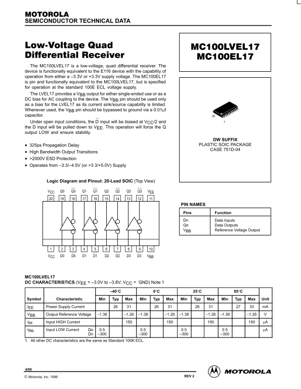
The MC100LVEL17 is a low-voltage, quad differential receiver. The device is functionally equivalent to the E116 device with the capability of operation from either a –3.3V or +3.3V supply voltage. The MC100EL17 is pin and functionally equivalent to the MC100LVEL17, but is specified for operation at the standard 100E ECL voltage supply. The LVEL17 provides a VBB output for either single-ended use or as a DC bias for AC coupling to the device. The VBB pin should be used only as a bias for the LVEL17 as its current sink/source capability is limited. Whenever used, the VBB pin should be bypassed to ground via a 0.01µf capacitor. Under open input conditions, the D input will be biased at VCC/2 and the D input will be pulled down to VEE. This operation will force the Q output LOW and ensure stability.
DW SUFFIX 325ps Propagation Delay PLASTIC SOIC PACKAGE CASE 751D-04
High Bandwidth Output Transitions >2000V ESD Protection Operates from –3.3/–4.5V (or +3.3/+5.0V) Supply
Logic Diagram and Pinout: 20-Lead SOIC (Top View)
VCC Q0 Q0 Q1 Q1 Q2 Q2 Q3 Q3 VEE
PIN NAMES
Pins Function Dn Data Inputs Qn Data Outputs VBB Reference Voltage Output
D0 D0 D1 D1 D2VCC D2 D3 D3 VBB
MC100LVEL17 DC CHARACTERISTICS (VEE = –3.0V to –3.8V; VCC = GND) Note 1
Symbol Characteristic Min Typ Max Min Typ Max Min Typ Max Min Typ Max Unit IEE Power Supply Current m A VBB Output Reference Voltage –1.38 –1.26 –1.38 –1.26 –1.38 –1.26 –1.38 –1.26 IIH Input HIGH Current µA IINL Input LOW Current Dn 0.5 0.5 0.5 0.5 µA
Dn –300 –300 –300 –300
1. All other DC characteristics are the same as Standard 100K ECL.
4–1 REV 2 Motorola, Inc. 1996
Page Summary Contents For Motorola MC100EL17 MC100LVEL17 User Guide (1)
Manual Details
| Brand | Motorola |
|---|---|
| Pages | 4 |
| File Size | 67.03 KB |
| Published | May 31, 2026 |
Enter the captcha to get the download link:

Frequently Asked Questions
How should I properly connect the 'V' output pin?
The V pin must be used only as a bias and always bypassed to ground via a 0.01μf capacitor.
Does this receiver support both +3.3V and -3.3V supply voltages?
Yes, the MC100LVEL17 is functionally equivalent to E116 and can operate from either a –3.3V or +3.3V supply voltage.
What are the typical output rise and fall times (t_r/t_f)?
The minimum typical differential output rise/fall time ranges between 280 ps and 550 ps.