MAXIM MAX9173 Quad LVDS Line Receiver with Flow-Through Pinout and "In-Path" Fail-Safe User Manual Data Sheet
Summary
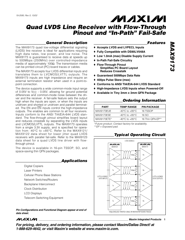
The MAX9173 is a high-speed Quad LVDS Line Receiver designed for reliable data signal processing up to 500Mbps. It accepts four differential LVDS inputs and converts them to standardized LVCMOS/LVTTL outputs, simplifying professional PCB layout with its flow-through pinout and incorporating an 'in-path' fail-safe circuit. This device is essential for electronics designers building sophisticated equipment such as network switches, digital copiers, laser printers, and telecom systems that require high-integrity, low-noise signal handling conforming to ANSI TIA/EIA-644 standards.
Page 1 Text Content
19-2595; Rev 0; 10/02
Quad LVDS Line Receiver with Flow-Through
Pinout and “In-Path” Fail-Safe
General Description Features
The MAX9173 quad low-voltage differential signaling Accepts LVDS and LVPECL Inputs (LVDS) line receiver is ideal for applications requiring
Fully Compatible with DS90LV048A
high data rates, low power, and low noise. The
Low 1.0m A (max) Disable Supply Current
MAX9173 is guaranteed to receive data at speeds up to 500Mbps (250MHz) over controlled-impedance In-Path Fail-Safe Circuitry media of approximately 100Ω. The transmission media
Flow-Through Pinout
can be printed circuit (PC) board traces or cables.
Simplifies PC Board Layout
The MAX9173 accepts four LVDS differential inputs and Reduces Crosstalk translates them to LVCMOS/LVTTL outputs. The
Guaranteed 500Mbps Data Rate
MAX9173 inputs are high impedance and require an
400ps Pulse Skew (max)
external termination resistor when used in a point-to- point connection. Conforms to ANSI TIA/EIA-644 LVDS Standard The device supports a wide common-mode input range High-Impedance LVDS Inputs when Powered-Off
of 0.05V to VCC - 0.05V, allowing for ground potential
Available in Tiny 3mm x 3mm QFN Package
differences and common-mode noise between the dri- ver and the receiver. A fail-safe feature sets the output
Ordering Information
high when the inputs are open, or when the inputs are undriven and shorted or undriven and parallel terminat-
PART TEMP RANGE PIN-PACKAGE
ed. The EN and EN inputs control the high-impedance
outputs. The enables are common to all four receivers. MAX9173EUE -40°C to +85°C 16 TSSOP
Inputs conform to the ANSI TIA/EIA-644 LVDS stan- MAX9173ESE -40°C to +85°C 16 SO dard. The flow-through pinout simplifies board layout
MAX9173ETE* -40°C to +85°C 16 Thin QFN-EP**
and reduces crosstalk by separating the LVDS inputs
and LVCMOS/LVTTL outputs. The MAX9173 operates *Future product. Contact factory for availability. **EP = Exposed pad.
from a single 3.3V supply, and is specified for opera- tion from -40°C to +85°C. Refer to the MAX9121/ MAX9122 data sheet for lower j itter quad LVDS
Typical Operating Circuit
receivers with parallel fail-safe. Refer to the MAX9123 data sheet for a quad LVDS line driver with flow- LVDS SIGNALS through pinout.
MAX9123 MAX9173
The device is available in 16-pin TSSOP, SO, and space-saving thin QFN packages.
Tx 100Ω Rx
Applications
Digital Copiers
Tx 100Ω Rx
Laser Printers Cellular Phone Base Stations
LVTTL/LVCMOS LVTTL/LVCMOS DATA INPUTS DATA OUTPUTS
Network Switches/Routers Backplane Interconnect
Tx 100Ω Rx
Clock Distribution LCD Displays Telecom Switching Equipment
Tx 100Ω Rx
Pin Configurations and Functional Diagram appear at end of
100Ω SHIELDED TWISTED CABLE OR MICROSTRIP BOARD TRACES
data sheet.
Maxim Integrated Products
For pricing, delivery, and ordering information, please contact Maxim/Dallas Direct! at 1-888-629-4642, or visit Maxim’s website at www.maxim-ic.com.
Page Summary Contents For MAXIM MAX9173 Quad LVDS Line Receiver with Flow-Through Pinout and "In-Path" Fail-Safe User Manual Data Sheet
Manual Details
| Brand | QUAD |
|---|---|
| Pages | 14 |
| File Size | 340.76 KB |
| Published | May 29, 2026 |
Enter the captcha to get the download link:

Frequently Asked Questions
What is the maximum guaranteed data rate of this receiver?
The MAX9173 is guaranteed to receive data at speeds up to 500Mbps.
Does the flow-through pinout simplify PCB design?
Yes, it simplifies PC Board Layout and helps reduce crosstalk.
Is an external termination resistor required for operation?
Yes, a 400ps Pulse Skew (max) external termination resistor is needed in point-to-point connections.
What does the 'In-Path' fail-safe circuit do?
It maintains safe output by detecting open, undriven/shorted, or parallel terminated inputs.