MAXIM MAX21458DK Quad T1/E1/J1 Transceiver Design Kit Daughter Board Data Sheet User Manual
Summary
This evaluation development kit is designed for engineers testing the quad T1/E1/J1 transceiver functionality using the DS21458 chip. It provides a comprehensive platform with necessary transformers, network connectors, and protection circuitry, guaranteeing compatibility with major demo kits like DK101/DK2000. The accompanying documentation guides users through detailed system setup, register configuration via ChipView software, signal mapping, and implementing advanced features such as loss-of-signal detection. This kit is essential for communication professionals developing robust telecommunications infrastructure.
Page 1 Text Content
查询DS21458DK供应商
DS21458DK
Quad T1/E1/J1 Transceiver Design Kit Daughter Card
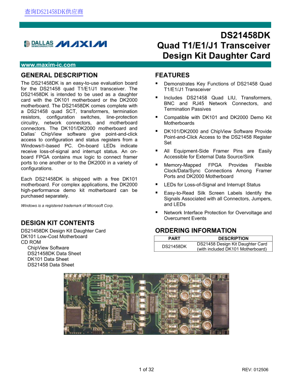
www.maxim-ic.com GENERAL DESCRIPTION FEATURES The DS21458DK is an easy-to-use evaluation board Demonstrates Key Functions of DS21458 Quad for the DS21458 quad T1/E1/J1 transceiver. The T1/E1/J1 Transceiver DS21458DK is intended to be used as a daughter
Includes DS21458 Quad LIU, Transformers,
card with the DK101 motherboard or the DK2000
BNC and RJ45 Network Connectors, and
motherboard. The DS21458DK comes complete with
Termination Passives
a DS21458 quad SCT, transformers, termination resistors, configuration switches, line-protection Compatible with DK101 and DK2000 Demo Kit circuitry, network connectors, and motherboard Motherboards connectors. The DK101/DK2000 motherboard and
DK101/DK2000 and Chip View Software Provide
Dallas’ Chip View software give point-and-click
Point-and-Click Access to the DS21458 Register
access to configuration and status registers from a
Windows-based PC. On-board LEDs indicate
receive loss-of-signal and interrupt status. An on- All Equipment-Side Framer Pins are Easily board FPGA contains mux logic to connect framer Accessible for External Data Source/Sink
ports to one another or to the DK2000 in a variety of
Memory-Mapped FPGA Provides Flexible
configurations.
Clock/Data/Sync Connections Among Framer Ports and DK2000 Motherboard
Each DS21458DK is shipped with a free DK101 motherboard. For complex applications, the DK2000 LEDs for Loss-of-Signal and Interrupt Status high-performance demo kit motherboard can be
Easy-to-Read Silk Screen Labels Identify the
purchased separately.
Signals Associated with all Connectors, Jumpers, Windows is a registered trademark of Microsoft Corp. and LEDs Network Interface Protection for Overvoltage and Overcurrent Events
DESIGN KIT CONTENTS DS21458DK Design Kit Daughter Card ORDERING INFORMATION DK101 Low-Cost Motherboard
PART DESCRIPTION
CD ROM
DS21458DK DS21458 Design Kit Daughter Card
Chip View Software (with included DK101 Motherboard) DS21458DK Data Sheet DK101 Data Sheet DS21458 Data Sheet
1 of 32 REV: 012506
Page Summary Contents For MAXIM MAX21458DK Quad T1/E1/J1 Transceiver Design Kit Daughter Board Data Sheet User Manual
Manual Details
| Brand | QUAD |
|---|---|
| Pages | 32 |
| File Size | 1.20 MB |
| Published | May 27, 2026 |
Enter the captcha to get the download link:

Frequently Asked Questions
What kind of boards are compatible with the DS21458DK design kit?
It is compatible with the DK101 and DK2000 Demo Kit motherboard circuitry, network connectors, and motherboards.
How can I monitor the configuration and status of the DS21458 chip?
Use Dallas’ ChipView software on a Windows-based PC to access the configuration and status registers via point-and-click interface.
Is external connection available for data sources?
Yes, all Equipment-Side Framer Pins are easily accessible for external Data Source/Sink boards or FPGAs.
What is provided in the default design kit contents?
The kit includes a free DK101 motherboard, transformers, termination passives, and line-protection components.